2N6249 Datasheet. Specs and Replacement
Type Designator: 2N6249 📄📄
Material of Transistor: Si
Polarity: NPN
Absolute Maximum Ratings
Maximum Collector Power Dissipation (Pc): 175 W
Maximum Collector-Base Voltage |Vcb|: 300 V
Maximum Collector-Emitter Voltage |Vce|: 200 V
Maximum Emitter-Base Voltage |Veb|: 6 V
Maximum Collector Current |Ic max|: 10 A
Max. Operating Junction Temperature (Tj): 200 °C
Electrical Characteristics
Transition Frequency (ft): 2.5 MHz
Forward Current Transfer Ratio (hFE), MIN: 10
Noise Figure, dB: -
Package: TO3
📄📄 Copy
- BJT ⓘ Cross-Reference Search
2N6249 datasheet
..1. Size:111K central
2n6249 2n6250 2n6251.pdf 

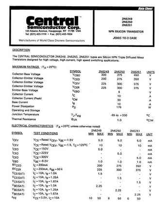
145 Adams Avenue, Hauppauge, NY 11788 USA Tel (631) 435-1110 Fax (631) 435-1824 TM Central Semiconductor Corp. 145 Adams Avenue Hauppauge, NY 11788 USA Tel (631) 435-1110 Fax (631) 435-1824 www.centralsemi.com ... See More ⇒
..2. Size:122K jmnic
2n6249 2n6250 2n6251.pdf 

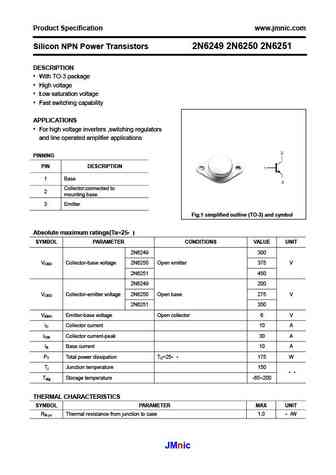
Product Specification www.jmnic.com Silicon NPN Power Transistors 2N6249 2N6250 2N6251 DESCRIPTION With TO-3 package High voltage Low saturation voltage Fast switching capability APPLICATIONS For high voltage inverters ,switching regulators and line operated amplifier applications PINNING PIN DESCRIPTION 1 Base Collector;connected to 2 mounting base 3 Em... See More ⇒
..3. Size:176K aeroflex
2n6249 2n6250 2n6251.pdf 

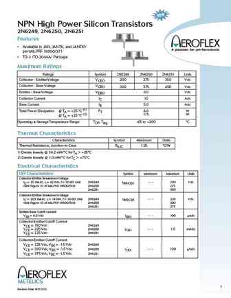
NPN High Power Silicon Transistors 2N6249, 2N6250, 2N6251 Features Available in JAN, JANTX, and JANTXV per MIL-PRF-19500/371 TO-3 (TO-204AA) Package Maximum Ratings Ratings Symbol 2N6249 2N6250 2N6251 Units Collector - Emitter Voltage VCEO 200 275 350 Vdc Collector - Base Voltage VCBO 300 375 450 Vdc Emitter - Base Voltage VEBO 6.0 Vdc Collector Current IC 10 Adc Base Curr... See More ⇒
..4. Size:119K inchange semiconductor
2n6249 2n6250 2n6251.pdf 
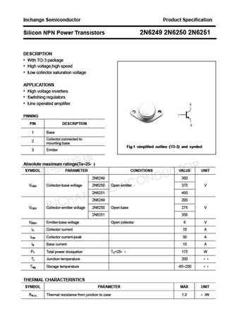
Inchange Semiconductor Product Specification Silicon NPN Power Transistors 2N6249 2N6250 2N6251 DESCRIPTION With TO-3 package High voltage,high speed Low collector saturation voltage APPLICATIONS High voltage inverters Switching regulators Line operated amplifier PINNING PIN DESCRIPTION 1 Base Collector;connected to 2 mounting base Fig.1 simplified out... See More ⇒
0.1. Size:382K comset
2n6249-2n6250-2n6251.pdf 

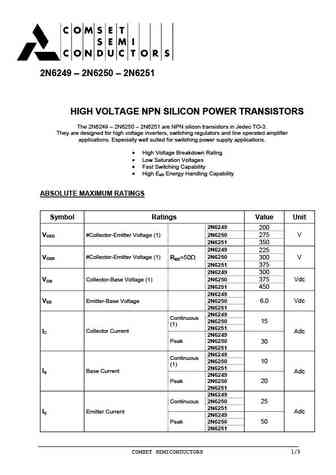
2N6249 2N6250 2N6251 HIGH VOLTAGE NPN SILICON POWER TRANSISTORS HIGH VOLTAGE NPN SILICON POWER TRANSISTORS The 2N6249 2N6250 2N6251 are NPN silicon transistors in Jedec TO-3. They are designed for high voltage inverters, switching regulators and line operated amplifier applications. Especially well suited for switching power supply applications. High Voltage Breakdown ... See More ⇒
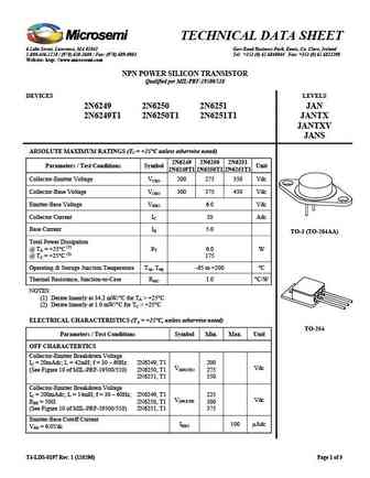
0.2. Size:179K microsemi
2n6249t1 2n6249t1 2n6250t1.pdf 

TECHNICAL DATA SHEET 6 Lake Street, Lawrence, MA 01841 Gort Road Business Park, Ennis, Co. Clare, Ireland 1-800-446-1158 / (978) 620-2600 / Fax (978) 689-0803 Tel +353 (0) 65 6840044 Fax +353 (0) 65 6822298 Website http //www.microsemi.com NPN POWER SILICON TRANSISTOR Qualified per MIL-PRF-19500/510 DEVICES LEVELS 2N6249 2N6250 2N6251 JAN 2N6249T1 2N6250T1 2N6251T1 JANTX JA... See More ⇒
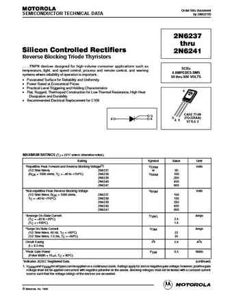
9.1. Size:96K motorola
2n6237 2n6238 2n6239 2n6240 2n6241.pdf 

MOTOROLA Order this document SEMICONDUCTOR TECHNICAL DATA by 2N6237/D 2N6237 thru Silicon Controlled Rectifiers 2N6241 Reverse Blocking Triode Thyristors . . . PNPN devices designed for high volume consumer applications such as SCRs temperature, light, and speed control; process and remote control, and warning 4 AMPERES RMS systems where reliability of operation is important. 50 t... See More ⇒
9.3. Size:11K semelab
2n6247.pdf 

2N6247 Dimensions in mm (inches). Bipolar PNP Device in a Hermetically sealed TO3 25.15 (0.99) 6.35 (0.25) 26.67 (1.05) 9.15 (0.36) Metal Package. 10.67 (0.42) 11.18 (0.44) 1.52 (0.06) 3.43 (0.135) 1 2 Bipolar PNP Device. 3 VCEO = 90V (case) 3.84 (0.151) 4.09 (0.161) 7.92 (0.312) IC = 10A 12.70 (0.50) All Semelab hermetically sealed products can be processed in a... See More ⇒
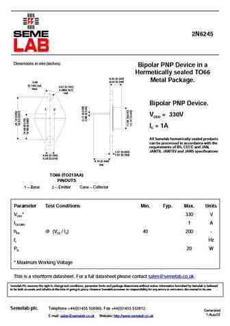
9.4. Size:10K semelab
2n6245.pdf 

2N6245 Dimensions in mm (inches). Bipolar PNP Device in a Hermetically sealed TO66 6.35 (0.250) Metal Package. 8.64 (0.340) 3.68 (0.145) rad. 3.61 (0.142) max. 4.08(0.161) rad. Bipolar PNP Device. 1 2 VCEO = 330V IC = 1A All Semelab hermetically sealed products can be processed in accordance with the requirements of BS, CECC and JAN, JANTX, JANTXV and JANS speci... See More ⇒
9.5. Size:11K semelab
2n6246.pdf 

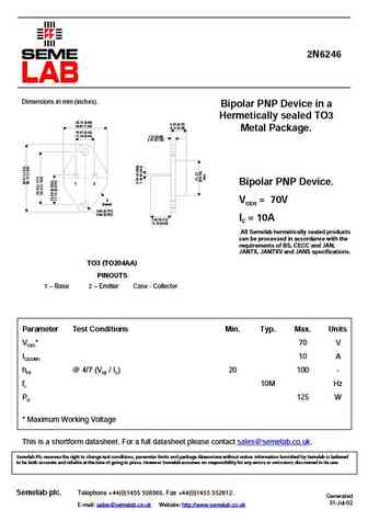
2N6246 Dimensions in mm (inches). Bipolar PNP Device in a Hermetically sealed TO3 25.15 (0.99) 6.35 (0.25) 26.67 (1.05) 9.15 (0.36) Metal Package. 10.67 (0.42) 11.18 (0.44) 1.52 (0.06) 3.43 (0.135) 1 2 Bipolar PNP Device. 3 VCEO = 70V (case) 3.84 (0.151) 4.09 (0.161) 7.92 (0.312) IC = 10A 12.70 (0.50) All Semelab hermetically sealed products can be processed in a... See More ⇒
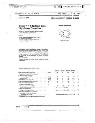
9.6. Size:122K jmnic
2n6246 2n6247 2n6248.pdf 

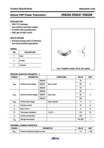
Product Specification www.jmnic.com Silicon PNP Power Transistors 2N6246 2N6247 2N6248 DESCRIPTION With TO-3 package Low collector saturation voltage Excellent safe operating area High gain at high current APPLICATIONS General-purpose types of switching and linear-amplifier applications PINNING PIN DESCRIPTION 1 Base 2 Emitter 3 Collector Fig.1 simplified ou... See More ⇒
9.7. Size:118K inchange semiconductor
2n6246 2n6247 2n6248.pdf 
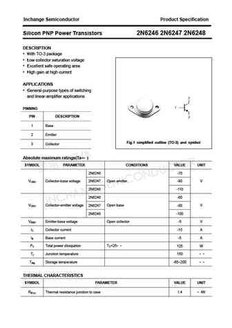
Inchange Semiconductor Product Specification Silicon PNP Power Transistors 2N6246 2N6247 2N6248 DESCRIPTION With TO-3 package Low collector saturation voltage Excellent safe operating area High gain at high current APPLICATIONS General-purpose types of switching and linear-amplifier applications PINNING PIN DESCRIPTION 1 Base 2 Emitter Fig.1 simplified outlin... See More ⇒
Detailed specifications: 2N6233, 2N6234, 2N6235, 2N6235R, 2N624, 2N6246, 2N6247, 2N6248, BC337, 2N625, 2N6250, 2N6251, 2N6253, 2N6254, 2N6255, 2N6256, 2N6257
Keywords - 2N6249 pdf specs
2N6249 cross reference
2N6249 equivalent finder
2N6249 pdf lookup
2N6249 substitution
2N6249 replacement
