2N626 Datasheet. Specs and Replacement
Type Designator: 2N626 📄📄
Material of Transistor: Si
Polarity: NPN
Absolute Maximum Ratings
Maximum Collector Power Dissipation (Pc): 10 W
Maximum Collector-Base Voltage |Vcb|: 30 V
Maximum Collector-Emitter Voltage |Vce|: 30 V
Maximum Emitter-Base Voltage |Veb|: 10 V
Maximum Collector Current |Ic max|: 3 A
Max. Operating Junction Temperature (Tj): 90 °C
Electrical Characteristics
Transition Frequency (ft): 0.2 MHz
Forward Current Transfer Ratio (hFE), MIN: 180000
Package: TO3
📄📄 Copy
2N626 Substitution
- BJT ⓘ Cross-Reference Search
2N626 datasheet
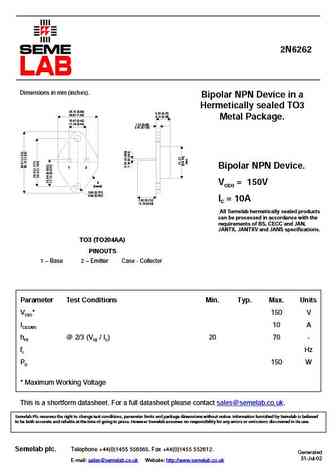
2N6262 Dimensions in mm (inches). Bipolar NPN Device in a Hermetically sealed TO3 25.15 (0.99) 6.35 (0.25) 26.67 (1.05) 9.15 (0.36) Metal Package. 10.67 (0.42) 11.18 (0.44) 1.52 (0.06) 3.43 (0.135) 1 2 Bipolar NPN Device. 3 VCEO = 150V (case) 3.84 (0.151) 4.09 (0.161) 7.92 (0.312) IC = 10A 12.70 (0.50) All Semelab hermetically sealed products can be processed in ... See More ⇒
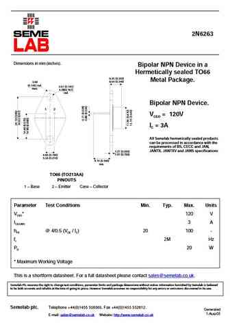
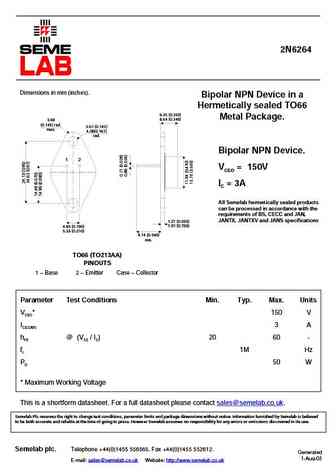
2N6263 Dimensions in mm (inches). Bipolar NPN Device in a Hermetically sealed TO66 6.35 (0.250) Metal Package. 8.64 (0.340) 3.68 (0.145) rad. 3.61 (0.142) max. 4.08(0.161) rad. Bipolar NPN Device. 1 2 VCEO = 120V IC = 3A All Semelab hermetically sealed products can be processed in accordance with the requirements of BS, CECC and JAN, JANTX, JANTXV and JANS speci... See More ⇒
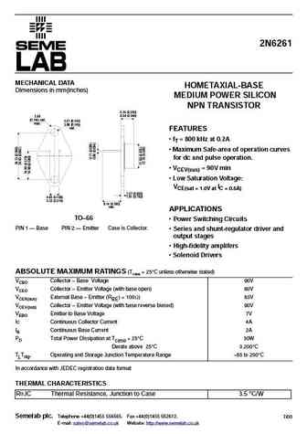
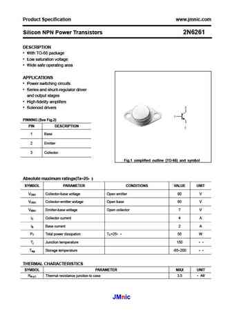
2N6261 MECHANICAL DATA HOMETAXIAL-BASE Dimensions in mm(inches) MEDIUM POWER SILICON NPN TRANSISTOR 6.35 (0.250) 8.64 (0.340) 3.68 (0.145) rad. 3.61 (0.142) max. 3.86 (0.145) rad. FEATURES fT = 800 kHz at 0.2A Maximum Safe-area of operation curves for dc and pulse operation. VCEV(sus) = 90V min Low Saturation Voltage VCE(sat = 1.0V at IC = 0.5A) 1.27 (0.050... See More ⇒
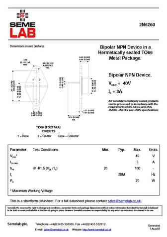
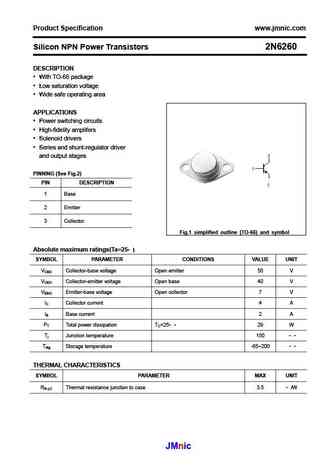
2N6260 Dimensions in mm (inches). Bipolar NPN Device in a Hermetically sealed TO66 6.35 (0.250) Metal Package. 8.64 (0.340) 3.68 (0.145) rad. 3.61 (0.142) max. 4.08(0.161) rad. Bipolar NPN Device. 1 2 VCEO = 40V IC = 3A All Semelab hermetically sealed products can be processed in accordance with the requirements of BS, CECC and JAN, JANTX, JANTXV and JANS specif... See More ⇒
Detailed specifications: 2N6251, 2N6253, 2N6254, 2N6255, 2N6256, 2N6257, 2N6258, 2N6259, 13009, 2N6260, 2N6261, 2N6262, 2N6263, 2N6264, 2N6265, 2N6266, 2N6267
Keywords - 2N626 pdf specs
2N626 cross reference
2N626 equivalent finder
2N626 pdf lookup
2N626 substitution
2N626 replacement
BJT Parameters and How They Relate
History: BDX53F | 2N3931 | QST5 | BUY56-4 | MUN2115T1G | DRA9143Z | CSB1086Q
🌐 : EN ES РУ
LIST
Last Update
BJT: ZDT6705 | GA1L4Z | GA1A4M | SBT42 | 2SA200-Y | 2SA200-O
Popular searches
3dd15d transistor | pa110bda | 2sb1243 | a1123 transistor | skd502t datasheet | svf7n65f | 2sc1419 datasheet | 2n4249 datasheet
