2N6266 Specs and Replacement
Type Designator: 2N6266
Material of Transistor: Si
Polarity: NPN
Absolute Maximum Ratings
Maximum Collector Power Dissipation (Pc): 14 W
Maximum Collector-Base Voltage |Vcb|: 50 V
Maximum Emitter-Base Voltage |Veb|: 3 V
Maximum Collector Current |Ic max|: 1 A
Max. Operating Junction Temperature (Tj): 200 °C
Electrical Characteristics
Transition Frequency (ft): 2000 MHz
Collector Capacitance (Cc): 10 pF
Forward Current Transfer Ratio (hFE), MIN: 5
Noise Figure, dB: -
Package: TO128
- BJT ⓘ Cross-Reference Search
2N6266 datasheet
9.1. Size:11K semelab
2n6262.pdf 
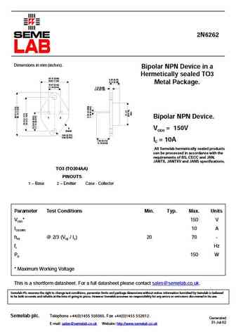
2N6262 Dimensions in mm (inches). Bipolar NPN Device in a Hermetically sealed TO3 25.15 (0.99) 6.35 (0.25) 26.67 (1.05) 9.15 (0.36) Metal Package. 10.67 (0.42) 11.18 (0.44) 1.52 (0.06) 3.43 (0.135) 1 2 Bipolar NPN Device. 3 VCEO = 150V (case) 3.84 (0.151) 4.09 (0.161) 7.92 (0.312) IC = 10A 12.70 (0.50) All Semelab hermetically sealed products can be processed in ... See More ⇒
9.2. Size:11K semelab
2n6263.pdf
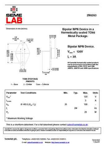
2N6263 Dimensions in mm (inches). Bipolar NPN Device in a Hermetically sealed TO66 6.35 (0.250) Metal Package. 8.64 (0.340) 3.68 (0.145) rad. 3.61 (0.142) max. 4.08(0.161) rad. Bipolar NPN Device. 1 2 VCEO = 120V IC = 3A All Semelab hermetically sealed products can be processed in accordance with the requirements of BS, CECC and JAN, JANTX, JANTXV and JANS speci... See More ⇒
9.3. Size:18K semelab
2n6261.pdf
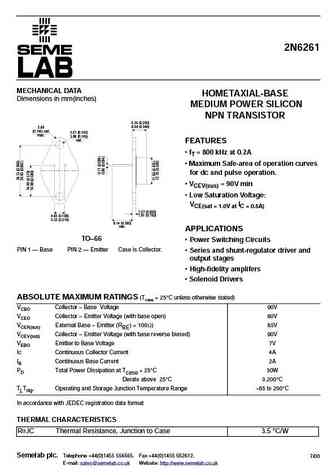
2N6261 MECHANICAL DATA HOMETAXIAL-BASE Dimensions in mm(inches) MEDIUM POWER SILICON NPN TRANSISTOR 6.35 (0.250) 8.64 (0.340) 3.68 (0.145) rad. 3.61 (0.142) max. 3.86 (0.145) rad. FEATURES fT = 800 kHz at 0.2A Maximum Safe-area of operation curves for dc and pulse operation. VCEV(sus) = 90V min Low Saturation Voltage VCE(sat = 1.0V at IC = 0.5A) 1.27 (0.050... See More ⇒
9.4. Size:11K semelab
2n6260.pdf
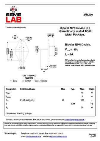
2N6260 Dimensions in mm (inches). Bipolar NPN Device in a Hermetically sealed TO66 6.35 (0.250) Metal Package. 8.64 (0.340) 3.68 (0.145) rad. 3.61 (0.142) max. 4.08(0.161) rad. Bipolar NPN Device. 1 2 VCEO = 40V IC = 3A All Semelab hermetically sealed products can be processed in accordance with the requirements of BS, CECC and JAN, JANTX, JANTXV and JANS specif... See More ⇒
9.5. Size:11K semelab
2n6264.pdf
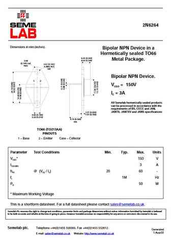
2N6264 Dimensions in mm (inches). Bipolar NPN Device in a Hermetically sealed TO66 6.35 (0.250) Metal Package. 8.64 (0.340) 3.68 (0.145) rad. 3.61 (0.142) max. 4.08(0.161) rad. Bipolar NPN Device. 1 2 VCEO = 150V IC = 3A All Semelab hermetically sealed products can be processed in accordance with the requirements of BS, CECC and JAN, JANTX, JANTXV and JANS speci... See More ⇒
9.6. Size:134K jmnic
2n6261.pdf
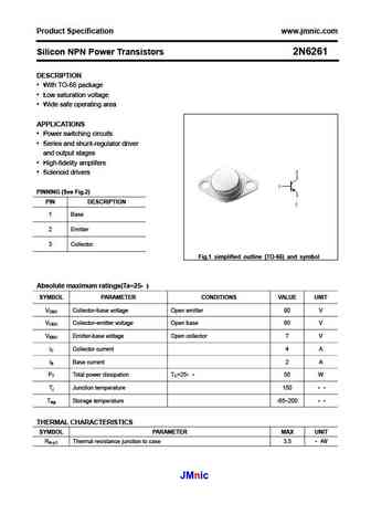
Product Specification www.jmnic.com Silicon NPN Power Transistors 2N6261 DESCRIPTION With TO-66 package Low saturation voltage Wide safe operating area APPLICATIONS Power switching circuits Series and shunt-regulator driver and output stages High-fidelity amplifers Solenoid drivers PINNING (See Fig.2) PIN DESCRIPTION 1 Base 2 Emitter 3 Collector Fig.... See More ⇒
9.7. Size:147K jmnic
2n6260.pdf
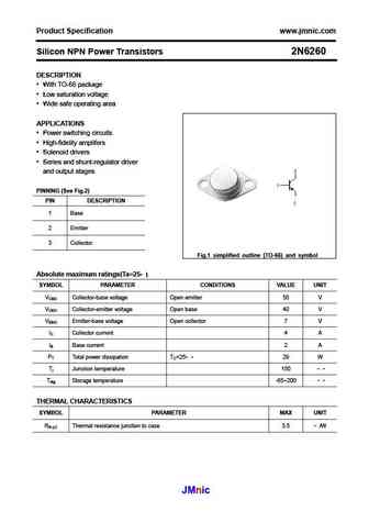
Product Specification www.jmnic.com Silicon NPN Power Transistors 2N6260 DESCRIPTION With TO-66 package Low saturation voltage Wide safe operating area APPLICATIONS Power switching circuits High-fidelity amplifers Solenoid drivers Series and shunt-regulator driver and output stages PINNING (See Fig.2) PIN DESCRIPTION 1 Base 2 Emitter 3 Collector Fig.... See More ⇒
9.8. Size:116K inchange semiconductor
2n6262.pdf
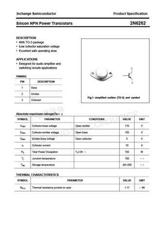
Inchange Semiconductor Product Specification Silicon NPN Power Transistors 2N6262 DESCRIPTION With TO-3 package Low collector saturation voltage Excellent safe operating area APPLICATIONS Designed for audio amplifier and switching circuits applications PINNING PIN DESCRIPTION 1 Base 2 Emitter Fig.1 simplified outline (TO-3) and symbol 3 Collector Absolute maxi... See More ⇒
9.9. Size:125K inchange semiconductor
2n6261.pdf
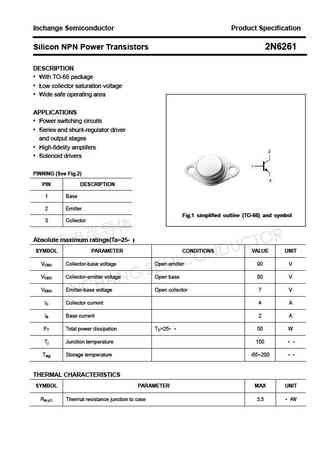
Inchange Semiconductor Product Specification Silicon NPN Power Transistors 2N6261 DESCRIPTION With TO-66 package Low collector saturation voltage Wide safe operating area APPLICATIONS Power switching circuits Series and shunt-regulator driver and output stages High-fidelity amplifers Solenoid drivers PINNING (See Fig.2) PIN DESCRIPTION 1 Base 2 Emitter... See More ⇒
9.10. Size:128K inchange semiconductor
2n6263 2n6264.pdf
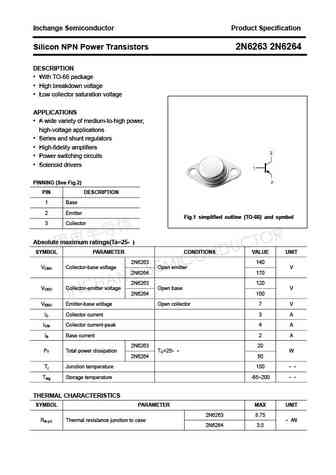
Inchange Semiconductor Product Specification Silicon NPN Power Transistors 2N6263 2N6264 DESCRIPTION With TO-66 package High breakdown voltage Low collector saturation voltage APPLICATIONS A wide variety of medium-to-high power, high-voltage applications Series and shunt regulators High-fidelity amplifiers Power switching circuits Solenoid drivers PINNI... See More ⇒
9.11. Size:125K inchange semiconductor
2n6260.pdf
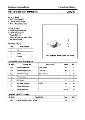
Inchange Semiconductor Product Specification Silicon NPN Power Transistors 2N6260 DESCRIPTION With TO-66 package Low saturation voltage Wide safe operating area APPLICATIONS Power switching circuits High-fidelity amplifers Solenoid drivers Series and shunt-regulator driver and output stages PINNING (See Fig.2) PIN DESCRIPTION 1 Base 2 Emitter Fig.1 si... See More ⇒
Detailed specifications: 2N6259, 2N626, 2N6260, 2N6261, 2N6262, 2N6263, 2N6264, 2N6265, 2SD1047, 2N6267, 2N6268, 2N6269, 2N627, 2N6270, 2N6271, 2N6272, 2N6273
Keywords - 2N6266 pdf specs
2N6266 cross reference
2N6266 equivalent finder
2N6266 pdf lookup
2N6266 substitution
2N6266 replacement
