5302 Specs and Replacement
Type Designator: 5302
Material of Transistor: Si
Polarity: NPN
Absolute Maximum Ratings
Maximum Collector Power Dissipation (Pc): 25 W
Maximum Collector-Base Voltage |Vcb|: 800 V
Maximum Collector-Emitter Voltage |Vce|: 400 V
Maximum Emitter-Base Voltage |Veb|: 10 V
Maximum Collector Current |Ic max|: 2 A
Max. Operating Junction Temperature (Tj): 150 °C
Electrical Characteristics
Forward Current Transfer Ratio (hFE), MIN: 10
Noise Figure, dB: -
Package: TO-251
- BJT ⓘ Cross-Reference Search
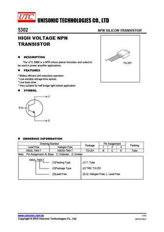
5302 datasheet
..1. Size:135K utc
5302.pdf 

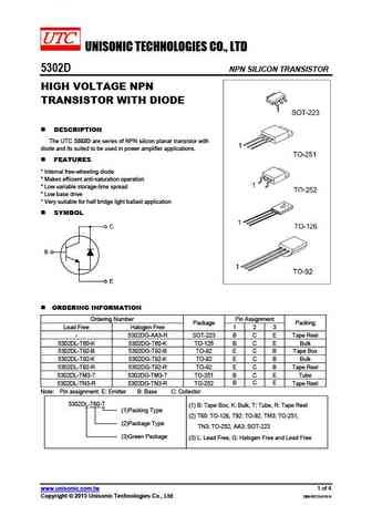
UNISONIC TECHNOLOGIES CO., LTD 5302 NPN SILICON TRANSISTOR HIGH VOLTAGE NPN TRANSISTOR DESCRIPTION 1 The UTC 5302 is a NPN silicon planar transistor and suited to TO-251 be used in power amplifier applications. FEATURES * Makes efficient anti-saturation operation * Low variable storage-time spread * Low base drive * Very suitable for half bridge light ballast applica... See More ⇒
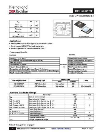
0.1. Size:240K 1
irfh5302trpbf.pdf 

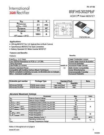
IRFH5302PbF HEXFET Power MOSFET VDS 30 V RDS(on) max 2.1 m (@VGS = 10V) Qg (typical) 29 nC RG (typical) 1.6 ID 100 A (@Tc(Bottom) = 25 C) PQFN 5X6 mm Applications OR-ing MOSFET for 12V (typical) Bus in-Rush Current Synchronous MOSFET for buck converters Battery Operated DC Motor Inverter MOSFET Features and Benefits Benefits Features ) Low RDSon (... See More ⇒
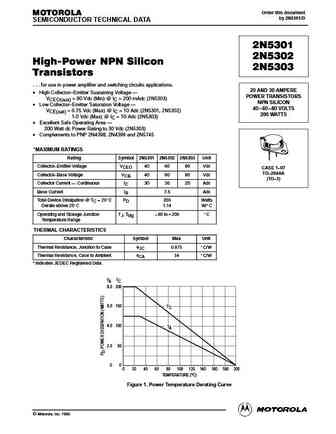
0.2. Size:251K motorola
2n5301 2n5302 2n5303.pdf 

Order this document MOTOROLA by 2N5301/D SEMICONDUCTOR TECHNICAL DATA 2N5301 2N5302 High-Power NPN Silicon 2N5303 Transistors . . . for use in power amplifier and switching circuits applications. 20 AND 30 AMPERE High Collector Emitter Sustaining Voltage POWER TRANSISTORS VCEO(sus) = 80 Vdc (Min) @ IC = 200 mAdc (2N5303) NPN SILICON Low Collector Emitter Saturatio... See More ⇒
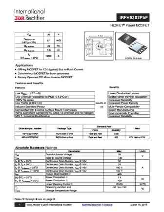
0.3. Size:240K international rectifier
irfh5302pbf.pdf 

IRFH5302PbF HEXFET Power MOSFET VDS 30 V RDS(on) max 2.1 m (@VGS = 10V) Qg (typical) 29 nC RG (typical) 1.6 ID 100 A (@Tc(Bottom) = 25 C) PQFN 5X6 mm Applications OR-ing MOSFET for 12V (typical) Bus in-Rush Current Synchronous MOSFET for buck converters Battery Operated DC Motor Inverter MOSFET Features and Benefits Benefits Features ) Low RDSon (... See More ⇒
0.4. Size:209K international rectifier
irfh5302.pdf 

PD -97156 IRFH5302PbF HEXFET Power MOSFET VDS 30 V RDS(on) max 2.1 m (@VGS = 10V) Qg (typical) 29 nC RG (typical) 1.6 ID 100 A (@Tc(Bottom) = 25 C) PQFN 5X6 mm Applications OR-ing MOSFET for 12V (typical) Bus in-Rush Current Synchronous MOSFET for buck converters Battery Operated DC Motor Inverter MOSFET Features and Benefits Benefits Features ... See More ⇒
0.5. Size:241K international rectifier
irfh5302dpbf.pdf 

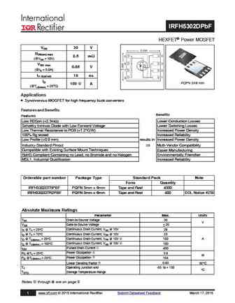
IRFH5302DPbF HEXFET Power MOSFET VDS 30 V RDS(on) max 2.5 m (@VGS = 10V) VSD max 0.65 V (@IS = 5.0A) trr (typical) 19 ns ID PQFN 5X6 mm 100 A (@Tc(Bottom) = 25 C) Applications Synchronous MOSFET for high frequency buck converters Features and Benefits Benefits Features Low RDSon (... See More ⇒
0.6. Size:89K sanyo
2sc5302.pdf 

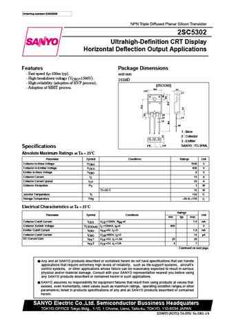
Ordering number EN5363B NPN Triple Diffused Planar Silicon Transistor 2SC5302 Ultrahigh-Definition CRT Display Horizontal Deflection Output Applications Features Package Dimensions Fast speed (tf=100ns typ). unit mm High breakdown voltage (VCBO=1500V). 2039D High reliability (adoption of HVP process). [2SC5302] Adoption of MBIT process. 16.0 5.6 3.4 3.1 2.8 2.0... See More ⇒
0.7. Size:92K onsemi
2n5302.pdf 

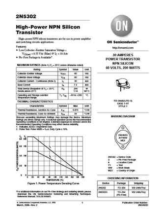
2N5302 High-Power NPN Silicon Transistor High-power NPN silicon transistors are for use in power amplifier and switching circuits applications. Features http //onsemi.com Low Collector-Emitter Saturation Voltage - VCE(sat) = 0.75 Vdc (Max) @ IC = 10 Adc 30 AMPERES Pb-Free Package is Available* POWER TRANSISTOR NPN SILICON MAXIMUM RATINGS (Note 1) (TJ = 25 C unless otherwis... See More ⇒
0.8. Size:92K onsemi
2n5302g.pdf 

2N5302 High-Power NPN Silicon Transistor High-power NPN silicon transistors are for use in power amplifier and switching circuits applications. Features http //onsemi.com Low Collector-Emitter Saturation Voltage - VCE(sat) = 0.75 Vdc (Max) @ IC = 10 Adc 30 AMPERES Pb-Free Package is Available* POWER TRANSISTOR NPN SILICON MAXIMUM RATINGS (Note 1) (TJ = 25 C unless otherwis... See More ⇒
0.9. Size:251K utc
5302d.pdf 

UNISONIC TECHNOLOGIES CO., LTD 5302D NPN SILICON TRANSISTOR HIGH VOLTAGE NPN TRANSISTOR WITH DIODE DESCRIPTION The UTC 5302D are series of NPN silicon planar transistor with diode and its suited to be used in power amplifier applications. FEATURES * Internal free-wheeling diode * Makes efficient anti-saturation operation * Low variable storage-time spread * Low bas... See More ⇒
0.10. Size:233K taiwansemi
tsc5302d.pdf 

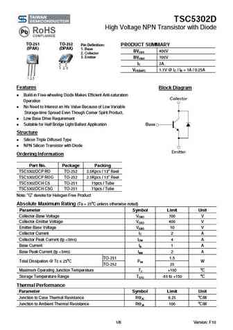
TSC5302D High Voltage NPN Transistor with Diode TO-251 TO-252 Pin Definition PRODUCT SUMMARY (IPAK) (DPAK) 1. Base BVCEO 400V 2. Collector 3. Emitter BVCBO 700V IC 2A VCE(SAT) 1.1V @ IC / IB = 1A / 0.25A Features Block Diagram Build-in Free-wheeling Diode Makes Efficient Anti-saturation Operation No Need to Interest an hfe Value Because of Low Variab... See More ⇒
0.11. Size:133K texas
csd25302q2.pdf 

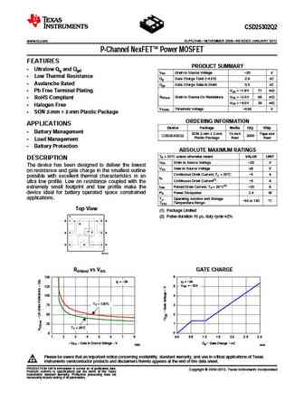
CSD25302Q2 www.ti.com SLPS234B NOVEMBER 2009 REVISED JANUARY 2012 P-Channel NexFET Power MOSFET 1 FEATURES PRODUCT SUMMARY Ultralow Qg and Qgd VDS Drain to Source Voltage 20 V Low Thermal Resistance Qg Gate Charge Total ( 4.5V) 2.6 nC Avalanche Rated Qgd Gate Charge Gate to Drain 0.5 nC VGS = 1.8V 71 m Pb Free Terminal Plating RDS(on) Drain to So... See More ⇒
0.12. Size:167K cn sptech
2n5302.pdf 

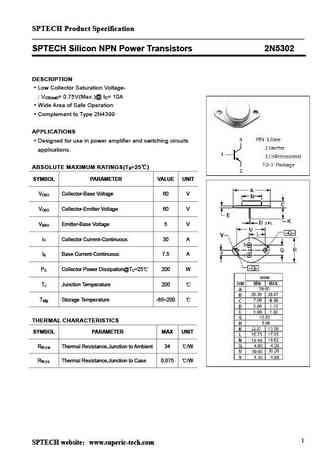
SPTECH Product Specification SPTECH Silicon NPN Power Transistors 2N5302 DESCRIPTION Low Collector Saturation Voltage- V = 0.75V(Max.)@ I = 10A CE(sat) C Wide Area of Safe Operation Complement to Type 2N4399 APPLICATIONS Designed for use in power amplifier and switching circuits applications. ABSOLUTE MAXIMUM RATINGS(T =25 ) a SYMBOL PARAMETER VALUE UNIT V Collector-Ba... See More ⇒
0.13. Size:196K inchange semiconductor
2n5302.pdf 
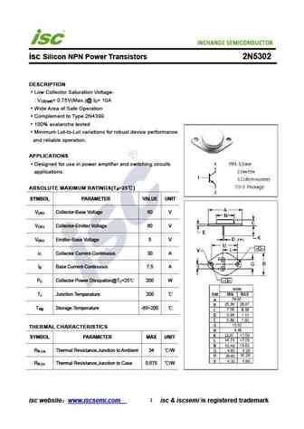
INCHANGE Semiconductor isc Silicon NPN Power Transistors 2N5302 DESCRIPTION Low Collector Saturation Voltage- V = 0.75V(Max.)@ I = 10A CE(sat) C Wide Area of Safe Operation Complement to Type 2N4399 100% avalanche tested Minimum Lot-to-Lot variations for robust device performance and reliable operation. APPLICATIONS Designed for use in power amplifier and switching cir... See More ⇒
0.14. Size:119K inchange semiconductor
2n5301 2n5302 2n5303.pdf 
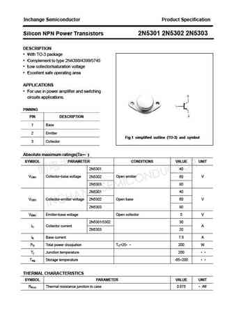
Inchange Semiconductor Product Specification Silicon NPN Power Transistors 2N5301 2N5302 2N5303 DESCRIPTION With TO-3 package Complement to type 2N4398/4399/5745 Low collector/saturation voltage Excellent safe operating area APPLICATIONS For use in power amplifier and switching circuits applications. PINNING PIN DESCRIPTION 1 Base 2 Emitter Fig.1 simplified o... See More ⇒
0.15. Size:211K inchange semiconductor
2sc5302.pdf 
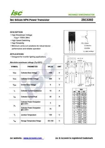
isc Silicon NPN Power Transistor 2SC5302 DESCRIPTION High Breakdown Voltage V = 1500V (Min) CBO High Speed Switching High Reliability Minimum Lot-to-Lot variations for robust device performance and reliable operation APPLICATIONS Designed for inverter lighting applications. Absolute maximum ratings (T =25 ) a SYMBOL PARAMETER VALUE UNIT V Collector-Base Voltage 1500 V... See More ⇒
Detailed specifications: SUT507EF, SUT509EF, SUT510EF, SUT562EF, SUT575EF, 4124, 4126, 4128, 2SC4793, 13002AH, 13003ADA, 13003BS, 13003DE, 13003DF, 13003DH, 13003DW, 13003EDA
Keywords - 5302 pdf specs
5302 cross reference
5302 equivalent finder
5302 pdf lookup
5302 substitution
5302 replacement
