2N646 Specs and Replacement
Type Designator: 2N646
Material of Transistor: Ge
Polarity: NPN
Absolute Maximum Ratings
Maximum Collector Power Dissipation (Pc): 0.1 W
Maximum Collector-Base Voltage |Vcb|: 25 V
Maximum Collector-Emitter Voltage |Vce|: 35 V
Maximum Emitter-Base Voltage |Veb|: 12 V
Maximum Collector Current |Ic max|: 0.05 A
Max. Operating Junction Temperature (Tj): 130 °C
Electrical Characteristics
Transition Frequency (ft): 40 MHz
Collector Capacitance (Cc): 4 pF
Forward Current Transfer Ratio (hFE), MIN: 50
Noise Figure, dB: -
Package: TO40
- BJT ⓘ Cross-Reference Search
2N646 datasheet
0.2. Size:11K semelab
2n6462.pdf 

2N6462 Dimensions in mm (inches). Bipolar NPN Device in a 8.51 (0.34) 9.40 (0.37) Hermetically sealed TO39 7.75 (0.305) 8.51 (0.335) Metal Package. 6.10 (0.240) 6.60 (0.260) Bipolar NPN Device. 0.89 max. (0.035) 12.70 (0.500) min. 0.41 (0.016) 0.53 (0.021) VCEO = 300V dia. IC = 0.1A 5.08 (0.200) typ. 2.54 All Semelab hermetically sealed products 2 (0.100) 1... See More ⇒
0.3. Size:11K semelab
2n6463.pdf

2N6463 Dimensions in mm (inches). Bipolar NPN Device in a 8.51 (0.34) 9.40 (0.37) Hermetically sealed TO39 7.75 (0.305) 8.51 (0.335) Metal Package. 6.10 (0.240) 6.60 (0.260) Bipolar NPN Device. 0.89 max. (0.035) 12.70 (0.500) min. 0.41 (0.016) 0.53 (0.021) VCEO = 250V dia. IC = 0.1A 5.08 (0.200) typ. 2.54 All Semelab hermetically sealed products 2 (0.100) 1... See More ⇒
0.4. Size:10K semelab
2n6465.pdf

2N6465 Dimensions in mm (inches). Bipolar NPN Device in a Hermetically sealed TO66 6.35 (0.250) Metal Package. 8.64 (0.340) 3.68 (0.145) rad. 3.61 (0.142) max. 4.08(0.161) rad. Bipolar NPN Device. 1 2 VCEO = 110V IC = 4A All Semelab hermetically sealed products can be processed in accordance with the requirements of BS, CECC and JAN, JANTX, JANTXV and JANS speci... See More ⇒
0.5. Size:10K semelab
2n6466.pdf

2N6466 Dimensions in mm (inches). Bipolar NPN Device in a Hermetically sealed TO66 6.35 (0.250) Metal Package. 8.64 (0.340) 3.68 (0.145) rad. 3.61 (0.142) max. 4.08(0.161) rad. Bipolar NPN Device. 1 2 VCEO = 130V IC = 4A All Semelab hermetically sealed products can be processed in accordance with the requirements of BS, CECC and JAN, JANTX, JANTXV and JANS speci... See More ⇒
0.6. Size:10K semelab
2n6468.pdf
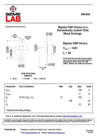
2N6468 Dimensions in mm (inches). Bipolar PNP Device in a Hermetically sealed TO66 6.35 (0.250) Metal Package. 8.64 (0.340) 3.68 (0.145) rad. 3.61 (0.142) max. 4.08(0.161) rad. Bipolar PNP Device. 1 2 VCEO = 130V IC = 4A All Semelab hermetically sealed products can be processed in accordance with the requirements of BS, CECC and JAN, JANTX, JANTXV and JANS speci... See More ⇒
0.7. Size:11K semelab
2n6461.pdf
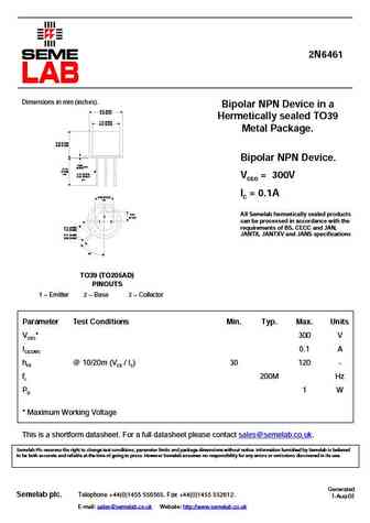
2N6461 Dimensions in mm (inches). Bipolar NPN Device in a 8.51 (0.34) 9.40 (0.37) Hermetically sealed TO39 7.75 (0.305) 8.51 (0.335) Metal Package. 6.10 (0.240) 6.60 (0.260) Bipolar NPN Device. 0.89 max. (0.035) 12.70 (0.500) min. 0.41 (0.016) 0.53 (0.021) VCEO = 300V dia. IC = 0.1A 5.08 (0.200) typ. 2.54 All Semelab hermetically sealed products 2 (0.100) 1... See More ⇒
0.8. Size:11K semelab
2n6464.pdf

2N6464 Dimensions in mm (inches). Bipolar NPN Device in a 8.51 (0.34) 9.40 (0.37) Hermetically sealed TO39 7.75 (0.305) 8.51 (0.335) Metal Package. 6.10 (0.240) 6.60 (0.260) Bipolar NPN Device. 0.89 max. (0.035) 12.70 (0.500) min. 0.41 (0.016) 0.53 (0.021) VCEO = 250V dia. IC = 0.1A 5.08 (0.200) typ. 2.54 All Semelab hermetically sealed products 2 (0.100) 1... See More ⇒
0.9. Size:10K semelab
2n6467.pdf

2N6467 Dimensions in mm (inches). Bipolar PNP Device in a Hermetically sealed TO66 6.35 (0.250) Metal Package. 8.64 (0.340) 3.68 (0.145) rad. 3.61 (0.142) max. 4.08(0.161) rad. Bipolar PNP Device. 1 2 VCEO = 110V IC = 4A All Semelab hermetically sealed products can be processed in accordance with the requirements of BS, CECC and JAN, JANTX, JANTXV and JANS speci... See More ⇒
0.10. Size:125K inchange semiconductor
2n6467 2n6468.pdf
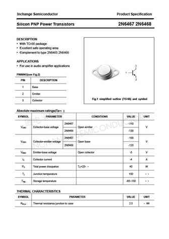
Inchange Semiconductor Product Specification Silicon PNP Power Transistors 2N6467 2N6468 DESCRIPTION With TO-66 package Excellent safe operating area Complement to type 2N6465 2N6466 APPLICATIONS For use in audio amplifier applications PINNING(see Fig.2) PIN DESCRIPTION 1 Base 2 Emitter Fig.1 simplified outline (TO-66) and symbol 3 Collector Absolute maximum rati... See More ⇒
0.11. Size:116K inchange semiconductor
2n6469.pdf
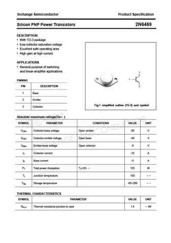
Inchange Semiconductor Product Specification Silicon PNP Power Transistors 2N6469 DESCRIPTION With TO-3 package Low collector saturation voltage Excellent safe operating area High gain at high current APPLICATIONS General-purpose of switching and linear-amplifier applications PINNING PIN DESCRIPTION 1 Base 2 Emitter Fig.1 simplified outline (TO-3) and symbol ... See More ⇒
0.12. Size:125K inchange semiconductor
2n6465 2n6466.pdf

Inchange Semiconductor Product Specification Silicon NPN Power Transistors 2N6465 2N6466 DESCRIPTION With TO-66 package Excellent safe operating area Complement to type 2N6467 2N6468 APPLICATIONS For use in audio amplifier applications PINNING(see Fig.2) PIN DESCRIPTION 1 Base 2 Emitter Fig.1 simplified outline (TO-66) and symbol 3 Collector Absolute maximum rat... See More ⇒
Detailed specifications: 2N6447, 2N6448, 2N645, 2N6455, 2N6456, 2N6457, 2N6458, 2N6459, A940, 2N6460, 2N6461, 2N6462, 2N6463, 2N6464, 2N6465, 2N6466, 2N6467
Keywords - 2N646 pdf specs
2N646 cross reference
2N646 equivalent finder
2N646 pdf lookup
2N646 substitution
2N646 replacement