2N6561 Specs and Replacement
Type Designator: 2N6561
Material of Transistor: Si
Polarity: NPN
Absolute Maximum Ratings
Maximum Collector Power Dissipation (Pc): 220 W
Maximum Collector-Base Voltage |Vcb|: 300 V
Maximum Collector-Emitter Voltage |Vce|: 300 V
Maximum Emitter-Base Voltage |Veb|: 5 V
Maximum Collector Current |Ic max|: 20 A
Max. Operating Junction Temperature (Tj): 200 °C
Electrical Characteristics
Transition Frequency (ft): 15 MHz
Forward Current Transfer Ratio (hFE), MIN: 10
Noise Figure, dB: -
Package: TO3
- BJT ⓘ Cross-Reference Search
2N6561 datasheet
..1. Size:12K semelab
2n6561.pdf 
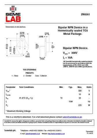
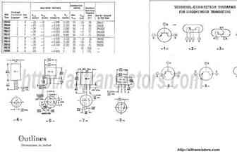
2N6561 Dimensions in mm (inches). Bipolar NPN Device in a Hermetically sealed TO3 25.15 (0.99) 6.35 (0.25) 26.67 (1.05) 9.15 (0.36) Metal Package. 10.67 (0.42) 11.18 (0.44) 1.52 (0.06) 3.43 (0.135) 1 2 Bipolar NPN Device. 3 VCEO = 300V (case) 3.84 (0.151) 4.09 (0.161) 7.92 (0.312) IC = 10A 12.70 (0.50) All Semelab hermetically sealed products can be processed in ... See More ⇒
..2. Size:217K inchange semiconductor
2n6561.pdf

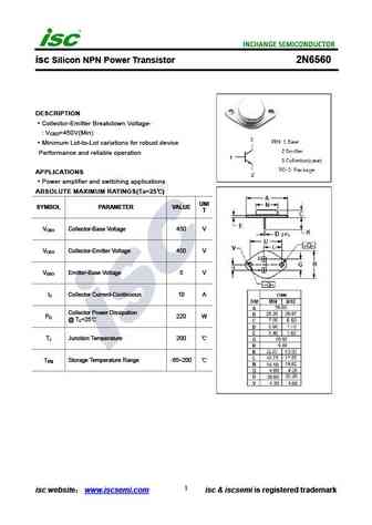
isc Silicon NPN Power Transistor 2N6561 DESCRIPTION Collector-Emitter Breakdown Voltage- V =300V(Min) CEO Minimum Lot-to-Lot variations for robust device Performance and reliable operation APPLICATIONS Power amplifier and switching applications ABSOLUTE MAXIMUM RATINGS(Ta=25 ) UNI SYMBOL PARAMETER VALUE T V Collector-Base Voltage 300 V CBO V Collector-Emitter Voltage 30... See More ⇒
9.3. Size:11K semelab
2n6560.pdf

2N6560 Dimensions in mm (inches). Bipolar NPN Device in a Hermetically sealed TO3 25.15 (0.99) 6.35 (0.25) 26.67 (1.05) 9.15 (0.36) Metal Package. 10.67 (0.42) 11.18 (0.44) 1.52 (0.06) 3.43 (0.135) 1 2 Bipolar NPN Device. 3 VCEO = 450V (case) 3.84 (0.151) 4.09 (0.161) 7.92 (0.312) IC = 10A 12.70 (0.50) All Semelab hermetically sealed products can be processed in ... See More ⇒
9.4. Size:150K jmnic
2n6569.pdf
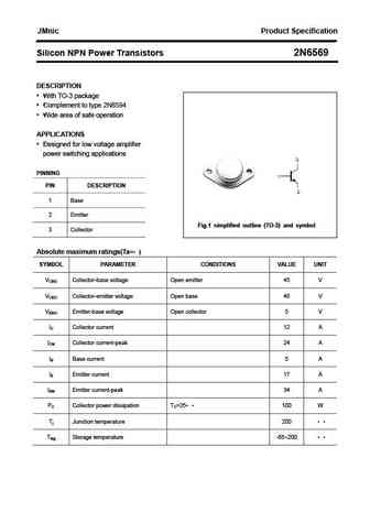
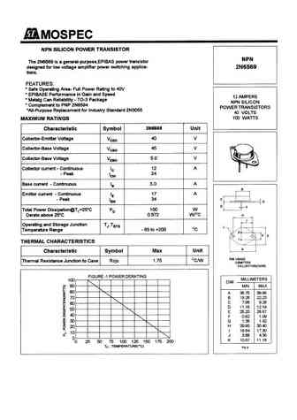
JMnic Product Specification Silicon NPN Power Transistors 2N6569 DESCRIPTION With TO-3 package Complement to type 2N6594 Wide area of safe operation APPLICATIONS Designed for low voltage amplifier power switching applications PINNING PIN DESCRIPTION 1 Base 2 Emitter Fig.1 simplified outline (TO-3) and symbol 3 Collector Absolute maximum ratings(Ta= ) SYMBO... See More ⇒
9.6. Size:217K inchange semiconductor
2n6560.pdf
isc Silicon NPN Power Transistor 2N6560 DESCRIPTION Collector-Emitter Breakdown Voltage- V =450V(Min) CEO Minimum Lot-to-Lot variations for robust device Performance and reliable operation APPLICATIONS Power amplifier and switching applications ABSOLUTE MAXIMUM RATINGS(Ta=25 ) UNI SYMBOL PARAMETER VALUE T V Collector-Base Voltage 450 V CBO V Collector-Emitter Voltage 45... See More ⇒
9.7. Size:117K inchange semiconductor
2n6569.pdf
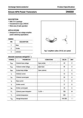
Inchange Semiconductor Product Specification Silicon NPN Power Transistors 2N6569 DESCRIPTION With TO-3 package Complement to type 2N6594 Wide area of safe operation APPLICATIONS Designed for low voltage amplifier power switching applications PINNING PIN DESCRIPTION 1 Base 2 Emitter Fig.1 simplified outline (TO-3) and symbol 3 Collector Absolute maximum rating... See More ⇒
Detailed specifications: 2N6554, 2N6555, 2N6556, 2N6557, 2N6558, 2N6559, 2N656, 2N6560, TIP127, 2N6562, 2N6563, 2N6566, 2N6567, 2N6569, 2N656A, 2N656S, 2N657
Keywords - 2N6561 pdf specs
2N6561 cross reference
2N6561 equivalent finder
2N6561 pdf lookup
2N6561 substitution
2N6561 replacement