2N6653 Specs and Replacement
Type Designator: 2N6653
Material of Transistor: Si
Polarity: NPN
Absolute Maximum Ratings
Maximum Collector Power Dissipation (Pc): 150 W
Maximum Collector-Base Voltage |Vcb|: 350 V
Maximum Collector-Emitter Voltage |Vce|: 300 V
Maximum Emitter-Base Voltage |Veb|: 7 V
Maximum Collector Current |Ic max|: 20 A
Max. Operating Junction Temperature (Tj): 175 °C
Electrical Characteristics
Transition Frequency (ft): 25 MHz
Collector Capacitance (Cc): 300 pF
Forward Current Transfer Ratio (hFE), MIN: 10
Package: TO3
2N6653 Substitution
- BJT ⓘ Cross-Reference Search
2N6653 datasheet
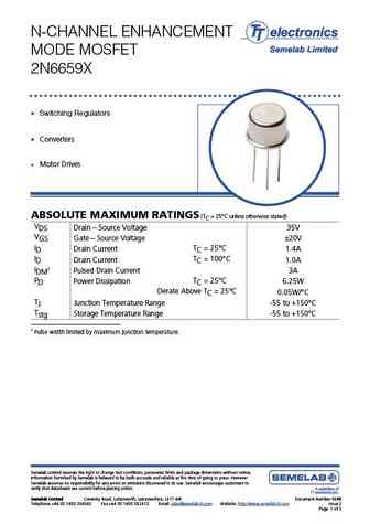
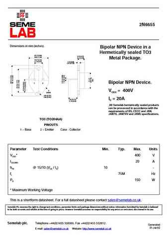
2N6653 Dimensions in mm (inches). Bipolar NPN Device in a Hermetically sealed TO3 25.15 (0.99) 6.35 (0.25) 26.67 (1.05) 9.15 (0.36) Metal Package. 10.67 (0.42) 11.18 (0.44) 1.52 (0.06) 3.43 (0.135) 1 2 Bipolar NPN Device. 3 VCEO = 300V (case) 3.84 (0.151) 4.09 (0.161) 7.92 (0.312) IC = 20A 12.70 (0.50) All Semelab hermetically sealed products can be processed in ... See More ⇒
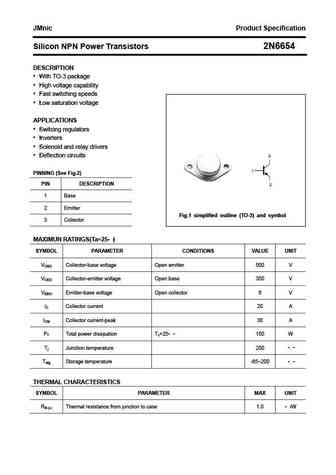
JMnic Product Specification Silicon NPN Power Transistors 2N6653 DESCRIPTION With TO-3 package High voltage capability Fast switching speeds Low saturation voltage APPLICATIONS Switcing regulators Inverters Solenoid and relay drivers Deflection circuits PINNING (See Fig.2) PIN DESCRIPTION 1 Base 2 Emitter Fig.1 simplified outline (TO-3) and symbol ... See More ⇒
isc Silicon NPN Power Transistor 2N6653 DESCRIPTION High Voltage Capability High Current Current Capability Low Collector Saturation Voltage- High Switching Speed Minimum Lot-to-Lot variations for robust device performance and reliable operation APPLICATIONS Desinged for use in switching and linear applications in military and power conversion. Absolute maximum ratings(Ta... See More ⇒
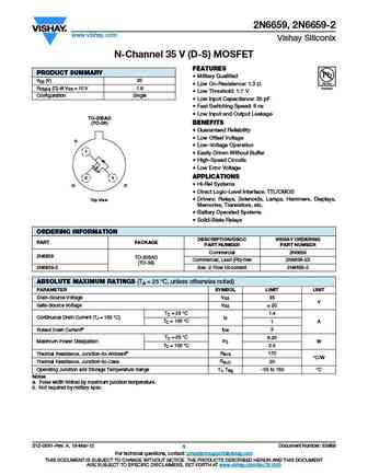
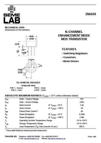
2N6659, 2N6659-2 www.vishay.com Vishay Siliconix N-Channel 35 V (D-S) MOSFET FEATURES PRODUCT SUMMARY Military Qualified VDS (V) 35 Low On-Resistence 1.3 RDS(on) ( ) at VGS = 10 V 1.8 Low Threshold 1.7 V Configuration Single Low Input Capacitance 35 pF Fast Switching Speed 8 ns Low Input and Output Leakage TO-205AD BENEFITS (TO-39) Guarant... See More ⇒
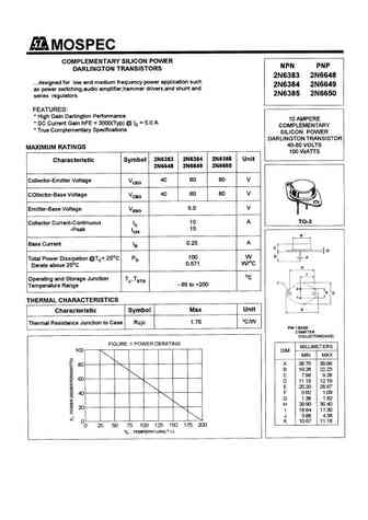
Detailed specifications: 2N6620, 2N6621, 2N6622, 2N663, 2N6648, 2N6649, 2N665, 2N6650, S8050, 2N6653-1, 2N6653-2, 2N6653-3, 2N6653A, 2N6653B, 2N6654, 2N6654-1, 2N6654-2
Keywords - 2N6653 pdf specs
2N6653 cross reference
2N6653 equivalent finder
2N6653 pdf lookup
2N6653 substitution
2N6653 replacement
🌐 : EN ES РУ
LIST
Last Update
BJT: GA1A4M | SBT42 | 2SA200-Y
Popular searches
bd140 transistor | 2n2222a datasheet | bd136 | tl431 datasheet | 2sd526 | 2n4403 transistor equivalent | 2sc1318 | 2n3055 transistor equivalent


