TB100 Specs and Replacement
Type Designator: TB100
Material of Transistor: Si
Polarity: NPN
Absolute Maximum Ratings
Maximum Collector Power Dissipation (Pc): 2 W
Maximum Collector-Base Voltage |Vcb|: 700 V
Maximum Collector-Emitter Voltage |Vce|: 700 V
Maximum Collector Current |Ic max|: 1 A
Max. Operating Junction Temperature (Tj): 150 °C
Electrical Characteristics
Forward Current Transfer Ratio (hFE), MIN: 14
Noise Figure, dB: -
Package: TO92
- BJT ⓘ Cross-Reference Search
TB100 datasheet
..1. Size:171K nxp
tb100.pdf 
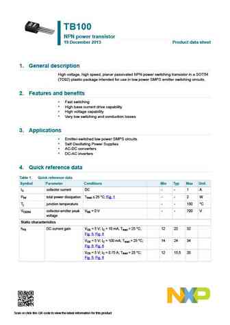
TB100 NPN power transistor 19 December 2013 Product data sheet 1. General description High voltage, high speed, planar passivated NPN power switching transistor in a SOT54 (TO92) plastic package intended for use in low power SMPS emitter switching circuits. 2. Features and benefits Fast switching High base current drive capability High voltage capability Very low switc... See More ⇒
..2. Size:248K cn ween semi
tb100.pdf
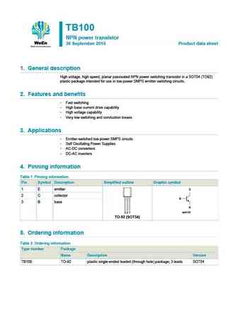
TB100 NPN power transistor 30 September 2016 Product data sheet 1. General description High voltage, high speed, planar passivated NPN power switching transistor in a SOT54 (TO92) plastic package intended for use in low power SMPS emitter switching circuits. 2. Features and benefits Fast switching High base current drive capability High voltage capability Very low swit... See More ⇒
0.1. Size:75K philips
mtb10010u 3.pdf
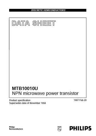
DISCRETE SEMICONDUCTORS DATA SHEET MTB10010U NPN microwave power transistor 1997 Feb 20 Product specification Supersedes data of November 1994 Philips Semiconductors Product specification NPN microwave power transistor MTB10010U FEATURES QUICK REFERENCE DATA Microwave performance for Tmb =25 C in a common base class C Input prematching cell allows an narrowband amplifier. ea... See More ⇒
0.3. Size:1657K st
stb100n10f7 std100n10f7 stf100n10f7 stf100n10f7 stp100n10f7.pdf
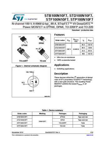
STB100N10F7, STD100N10F7, STF100N10F7, STP100N10F7 N-channel 100 V, 0.0068 typ., 80 A, STripFET VII DeepGATE Power MOSFET in D2PAK, DPAK, TO-220FP and TO-220 Datasheet - production data Features TAB TAB RDS(on) 3 Order codes VDS max ID PTOT 1 3 1 DPAK STB100N10F7 80 A 120 W D2PAK STD100N10F7 80 A 120W TAB 100 V 0.008 STF100N10F7 45 A 30 W STP100N10F7 80A 150 W ... See More ⇒
0.4. Size:395K st
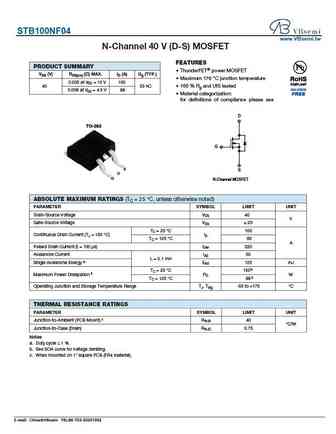
stb100nf04t4.pdf

STP100NF04 STB100NF04 N-channel 40V - 0.0043 - 120A - TO-220 - D2PAK STripFET II Power MOSFET General features Type VDSS RDS(on) ID Pw STP100NF04 40V ... See More ⇒
0.5. Size:338K st
stb100nf04l.pdf
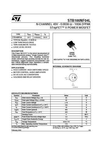
STB100NF04L N-CHANNEL 40V - 0.0036 - 100A D2PAK STripFET II POWER MOSFET TYPE VDSS RDS(on) ID STB100NF04L 40 V ... See More ⇒
0.6. Size:393K st
stb100nf03l.pdf
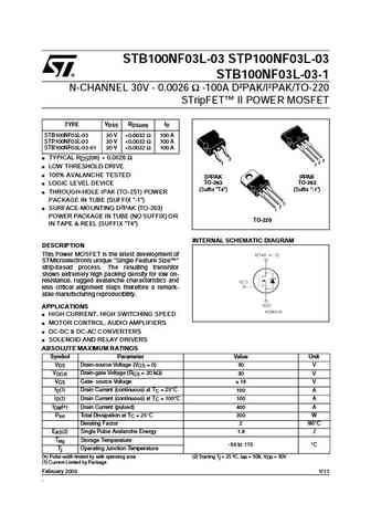
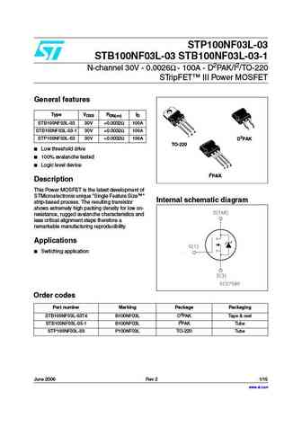
STB100NF03L-03 STP100NF03L-03 STB100NF03L-03-1 N-CHANNEL 30V - 0.0026 -100A D PAK/I PAK/TO-220 STripFET II POWER MOSFET TYPE VDSS RDS(on) ID STB100NF03L-03 30 V ... See More ⇒
0.7. Size:441K st
stb100nh02lt4.pdf

STB100NH02L N-channel 24V - 0.0052 - 60A - D2PAK STripFET III Power MOSFET General features Type VDSS RDS(on) ID STB100NH02L 24V ... See More ⇒
0.8. Size:398K st
stb100nf04 stp100nf04.pdf
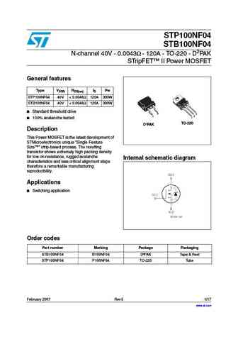
STP100NF04 STB100NF04 N-channel 40V - 0.0043 - 120A - TO-220 - D2PAK STripFET II Power MOSFET General features Type VDSS RDS(on) ID Pw STP100NF04 40V ... See More ⇒
0.9. Size:557K st
stb100n6f7.pdf
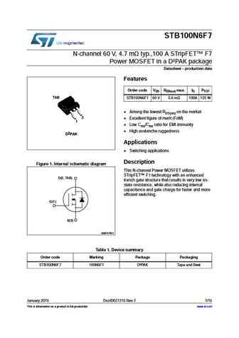
STB100N6F7 N-channel 60 V, 4.7 m typ.,100 A STripFET F7 Power MOSFET in a D PAK package Datasheet - production data Features Order code VDS RDS(on) max. ID PTOT TAB STB100N6F7 60 V 5.6 m 100A 125 W Among the lowest RDS(on) on the market 3 Excellent figure of merit (FoM) 1 Low Crss/Ciss ratio for EMI immunity High avalanche ruggedness D2PAK Applications ... See More ⇒
0.10. Size:648K st
stb100n10f7 std100n10f7 stf100n10f7 sti100n10f7 stp100n10f7.pdf
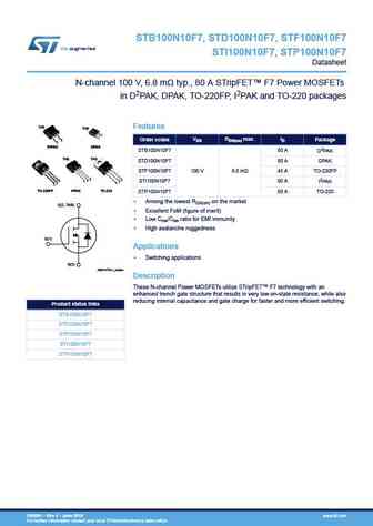
STB100N10F7, STD100N10F7, STF100N10F7 STI100N10F7, STP100N10F7 Datasheet N-channel 100 V, 6.8 m typ., 80 A STripFET F7 Power MOSFETs in D2PAK, DPAK, TO-220FP, I2PAK and TO-220 packages TAB TAB Features 2 3 1 VDS RDS(on) max. ID Order codes Package 3 1 D2PAK DPAK STB100N10F7 80 A D2PAK TAB TAB STD100N10F7 80 A DPAK STF100N10F7 100 V 8.0 m 45 A TO-220FP 3 3 2 3 1 2 ... See More ⇒
0.11. Size:450K st
stb100nh02l.pdf
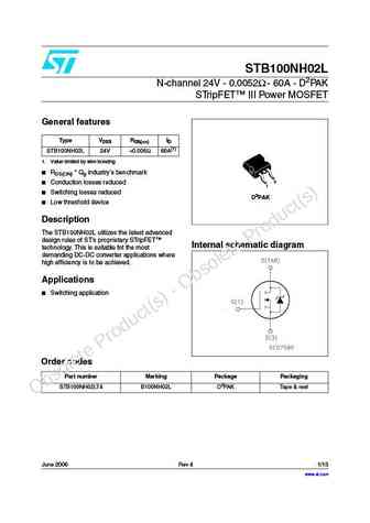
STB100NH02L N-channel 24V - 0.0052 - 60A - D2PAK STripFET III Power MOSFET General features Type VDSS RDS(on) ID STB100NH02L 24V ... See More ⇒
0.12. Size:106K onsemi
nstb1005dxv5.pdf
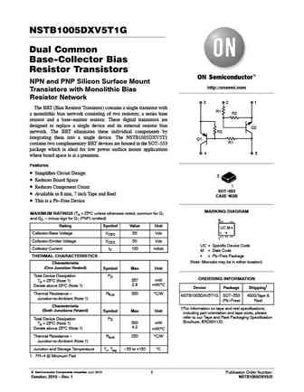
NSTB1005DXV5T1G Dual Common Base-Collector Bias Resistor Transistors NPN and PNP Silicon Surface Mount http //onsemi.com Transistors with Monolithic Bias Resistor Network 31 2 The BRT (Bias Resistor Transistor) contains a single transistor with R1 a monolithic bias network consisting of two resistors; a series base R2 resistor and a base-emitter resistor. These digital transistors ... See More ⇒
0.13. Size:63K onsemi
nstb1002dxv5.pdf
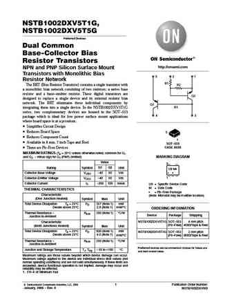
NSTB1002DXV5T1G, NSTB1002DXV5T5G Preferred Devices Dual Common Base-Collector Bias Resistor Transistors http //onsemi.com NPN and PNP Silicon Surface Mount Transistors with Monolithic Bias 31 2 Resistor Network R1 The BRT (Bias Resistor Transistor) contains a single transistor with R2 a monolithic bias network consisting of two resistors; a series base resistor and a base-emitter... See More ⇒
0.14. Size:63K onsemi
nstb1002dxv5-d.pdf

NSTB1002DXV5T1G, NSTB1002DXV5T5G Preferred Devices Dual Common Base-Collector Bias Resistor Transistors http //onsemi.com NPN and PNP Silicon Surface Mount Transistors with Monolithic Bias 31 2 Resistor Network R1 The BRT (Bias Resistor Transistor) contains a single transistor with R2 a monolithic bias network consisting of two resistors; a series base resistor and a base-emitter... See More ⇒
0.15. Size:1472K cn vbsemi
stb100nf04.pdf
STB100NF04 www.VBsemi.tw N-Channel 40 V (D-S) MOSFET FEATURES PRODUCT SUMMARY ThunderFET power MOSFET VDS (V) RDS(on) ( ) MAX. ID (A) Qg (TYP.) Maximum 175 C junction temperature 0.005 at VGS = 10 V 100 40 53 nC 100 % Rg and UIS tested 0.006 at VGS = 4.5 V 98 Material categorization for definitions of compliance please see D TO-263 G S S S D D G ... See More ⇒
0.16. Size:203K inchange semiconductor
stb100n10f7.pdf
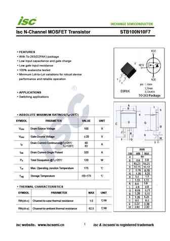
INCHANGE Semiconductor Isc N-Channel MOSFET Transistor STB100N10F7 FEATURES With To-263(D2PAK) package Low input capacitance and gate charge Low gate input resistance 100% avalanche tested Minimum Lot-to-Lot variations for robust device performance and reliable operation APPLICATIONS Switching applications ABSOLUTE MAXIMUM RATINGS(T =25 ) a SYMBOL PARAMETER VALU... See More ⇒
Detailed specifications: KTC9015SC, KTD1304S, KTA1297, KTA143ZKA, TA114ECA, TA124ECA, TA143ECA, TA144ECA, TIP120, TCC598, TCSA562O, TCSA562Y, KTA1267-GR, KTA1267-O, KTA1267-Y, KTA1270-O, KTA1270-Y
Keywords - TB100 pdf specs
TB100 cross reference
TB100 equivalent finder
TB100 pdf lookup
TB100 substitution
TB100 replacement