NSBC115TF3 Specs and Replacement
Type Designator: NSBC115TF3
SMD Transistor Code: P
Material of Transistor: Si
Polarity: Pre-Biased-NPN
Built in Bias Resistor R1 = 100 kOhm
Absolute Maximum Ratings
Maximum Collector Power Dissipation (Pc): 0.3 W
Maximum Collector-Base Voltage |Vcb|: 50 V
Maximum Collector-Emitter Voltage |Vce|: 50 V
Maximum Collector Current |Ic max|: 0.1 A
Max. Operating Junction Temperature (Tj): 150 °C
Electrical Characteristics
Forward Current Transfer Ratio (hFE), MIN: 160
Package: SOT1123-3
NSBC115TF3 Substitution
- BJT ⓘ Cross-Reference Search
NSBC115TF3 datasheet
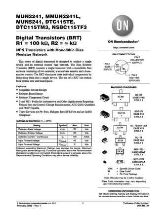
MUN2241, MMUN2241L, MUN5241, DTC115TE, DTC115TM3, NSBC115TF3 Digital Transistors (BRT) R1 = 100 kW, R2 = 8 kW http //onsemi.com NPN Transistors with Monolithic Bias PIN CONNECTIONS Resistor Network PIN 3 COLLECTOR This series of digital transistors is designed to replace a single (OUTPUT) PIN 1 device and its external resistor bias network. The Bias Resistor R1 BASE Transistor (... See More ⇒
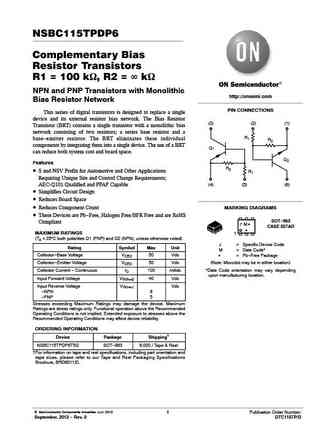
NSBC115TPDP6 Complementary Bias Resistor Transistors R1 = 100 kW, R2 = 8 kW NPN and PNP Transistors with Monolithic http //onsemi.com Bias Resistor Network PIN CONNECTIONS This series of digital transistors is designed to replace a single device and its external resistor bias network. The Bias Resistor (3) (2) (1) Transistor (BRT) contains a single transistor with a monolithic bias ... See More ⇒
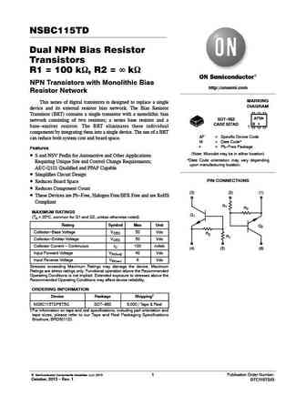
NSBC115TD Dual NPN Bias Resistor Transistors R1 = 100 kW, R2 = 8 kW NPN Transistors with Monolithic Bias http //onsemi.com Resistor Network MARKING This series of digital transistors is designed to replace a single DIAGRAM device and its external resistor bias network. The Bias Resistor Transistor (BRT) contains a single transistor with a monolithic bias AFMG SOT-963 network cons... See More ⇒
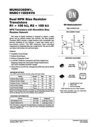
MUN5236DW1, NSBC115EDXV6 Dual NPN Bias Resistor Transistors R1 = 100 kW, R2 = 100 kW http //onsemi.com NPN Transistors with Monolithic Bias PIN CONNECTIONS Resistor Network (3) (2) (1) This series of digital transistors is designed to replace a single device and its external resistor bias network. The Bias Resistor R1 R2 Transistor (BRT) contains a single transistor with a monolith... See More ⇒
Detailed specifications: NSBC114YPDP6T5G, NSBC114YPDXV6, NSBC114YPDXV6T1G, NSBC114YPDXV6T5G, NSBC115EDXV6, NSBC115EDXV6T1G, NSBC115TDP6, NSBC115TDP6T5G, SS8050, NSBC115TF3T5G, NSBC115TPDP6, NSBC115TPDP6T5G, NSVBCX17LT1G, NSVBSP19AT1G, NSVBSS63LT1G, NSVBT2222ADW1T1G, NSVEMC2DXV5T1G
Keywords - NSBC115TF3 pdf specs
NSBC115TF3 cross reference
NSBC115TF3 equivalent finder
NSBC115TF3 pdf lookup
NSBC115TF3 substitution
NSBC115TF3 replacement
