H400S Specs and Replacement
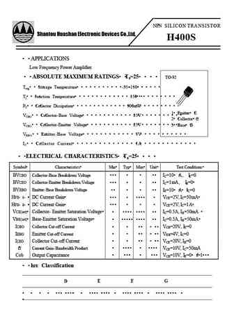
Type Designator: H400S
Material of Transistor: Si
Polarity: NPN
Absolute Maximum Ratings
Maximum Collector Power Dissipation (Pc): 0.9 W
Maximum Collector-Base Voltage |Vcb|: 25 V
Maximum Collector-Emitter Voltage |Vce|: 25 V
Maximum Emitter-Base Voltage |Veb|: 5 V
Maximum Collector Current |Ic max|: 1 A
Max. Operating Junction Temperature (Tj): 150 °C
Electrical Characteristics
Transition Frequency (ft): 180 typ MHz
Collector Capacitance (Cc): 15 pF
Forward Current Transfer Ratio (hFE), MIN: 60
Package: TO92
H400S Substitution
- BJT ⓘ Cross-Reference Search
H400S datasheet
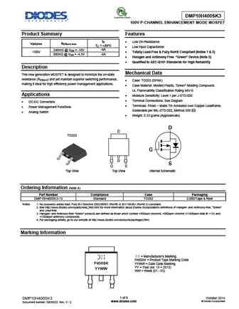
DMP10H400SK3 100V P-CHANNEL ENHANCEMENT MODE MOSFET Product Summary Features ID Low On-Resistance V(BR)DSS RDS(on) max TC = +25 C Low Input Capacitance 240m @ VGS = -10V -9A -100V Totally Lead-Free & Fully RoHS Compliant (Notes 1 & 2) -8A 300m @ VGS = -4.5V Halogen and Antimony Free. Green Device (Note 3) Qualified to AEC-Q101 Standards... See More ⇒
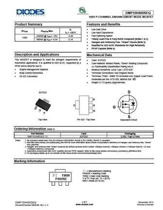
DMP10H400SEQ 100V P-CHANNEL ENHANCEMENT MODE MOSFET Product Summary Features and Benefits ID Low Gate Drive BVDSS RDS(ON) Max TA = +25 C Low Input Capacitance Fast Switching Speed 250m @ VGS = -10V -2.3A -100V Totally Lead-Free & Fully RoHS Compliant (Notes 1 & 2) 300m @ VGS = -4.5V -2.1A Halogen and Antimony Free. Green Device (Note 3) ... See More ⇒
Detailed specifications: H3332, H337, H368, H369, H370, H380TM, H3904, H3906, TIP42, H420, H421, H422, H423, H5342, H5401, H546, H547
Keywords - H400S pdf specs
H400S cross reference
H400S equivalent finder
H400S pdf lookup
H400S substitution
H400S replacement
History: 2SB1184 | 2SB1186 | HA7540 | BDS20 | BDT56 | 2SC3249 | 2SA1338-5
🌐 : EN ES РУ
LIST
Last Update
BJT: GA1A4M | SBT42 | 2SA200-Y | 2SA200-O | 2SD882-Q | 2SD882-P
Popular searches
2n404 | 2n4250 | d882 transistor equivalent | 17n80c3 | bc107 transistor | rjp63g4 datasheet | 2sc1115 | c3998 transistor


