SD1490 Specs and Replacement
Type Designator: SD1490
Material of Transistor: Si
Polarity: NPN
Absolute Maximum Ratings
Maximum Collector Power Dissipation (Pc): 155 W
Maximum Collector-Base Voltage |Vcb|: 45 V
Maximum Collector-Emitter Voltage |Vce|: 30 V
Maximum Emitter-Base Voltage |Veb|: 3 V
Maximum Collector Current |Ic max|: 8 A
Max. Operating Junction Temperature (Tj): 200 °C
Electrical Characteristics
Transition Frequency (ft): 860 MHz
Collector Capacitance (Cc): 72 pF
Forward Current Transfer Ratio (hFE), MIN: 10
Noise Figure, dB: -
Package: 450-BAL-FLG
- BJT ⓘ Cross-Reference Search
SD1490 datasheet
..1. Size:91K st
sd1490.pdf 

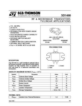
SD1490 RF & MICROWAVE TRANSISTORS TV/LINEAR APPLICATIONS .470 - 860 MHz .28 VOLTS .CLASS A PUSH PULL .DESIGNED FOR HIGH POWER LINEAR OPERATION .HIGH SATURATED POWER CAPABILITY .GOLD METALLIZATION .438 x .450 2LFL (M173) .DIFFUSED EMITTER BALLAST epoxy sealed RESISTORS ORDER CODE BRANDING .COMMON EMITTER CONFIGURATION SD1490 SD1490 .INTERNAL INPUT MATCHING .P 25 W MIN. WITH 9.0... See More ⇒
..2. Size:195K syntez microelectronics
sd1490.pdf 

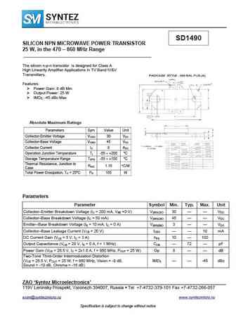
SD1490 SILICON NPN MICROWAVE POWER TRANSISTOR 25 W, in the 470 860 MHz Range ________________________________________________ The silicon n-p-n transistor is designed for Class A High Linearity Amplifier Applications in TV Band IV&V Transmitters. Features Power Gain 8 dB Min Output Power 25 W IMD3 -45 dBc Max Absolute Maximum Ratings Parameters Sym Value Unit Coll... See More ⇒
0.1. Size:23K hitachi
2sd1490.pdf 

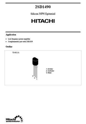
2SD1490 Silicon NPN Epitaxial Application Low frequency power amplifier Complementary pair with 2SB1059 Outline TO-92 (1) 1. Emitter 2. Collector 3. Base 3 2 1 2SD1490 Absolute Maximum Ratings (Ta = 25 C) Item Symbol Ratings Unit Collector to base voltage VCBO 70 V Collector to emitter voltage VCEO 50 V Emitter to base voltage VEBO 6V Collector current IC 1A Collec... See More ⇒
9.1. Size:97K st
sd1492.pdf 

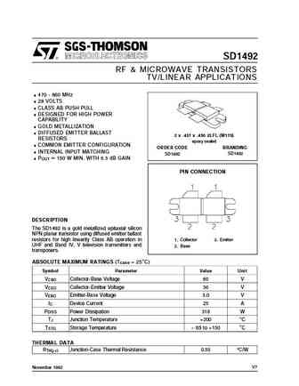
SD1492 RF & MICROWAVE TRANSISTORS TV/LINEAR APPLICATIONS .470 - 860 MHz .28 VOLTS .CLASS AB PUSH PULL .DESIGNED FOR HIGH POWER CAPABILITY .GOLD METALLIZATION .DIFFUSED EMITTER BALLAST 2 x .437 x .450 2LFL (M175) RESISTORS epoxy sealed .COMMON EMITTER CONFIGURATION ORDER CODE BRANDING .INTERNAL INPUT MATCHING SD1492 SD1492 .P 150 W MIN. WITH 6.5 dB GAIN = OUT PIN CONNECTION ... See More ⇒
9.2. Size:439K mcc
2sd1499-p.pdf 

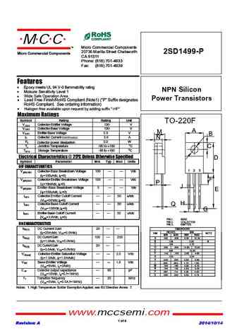
MCC TM Micro Commercial Components 20736 Marilla Street Chatsworth 2SD1499-P Micro Commercial Components CA 91311 Phone (818) 701-4933 Fax (818) 701-4939 Features Epoxy meets UL 94 V-0 flammability rating NPN Silicon Moisure Sensitivity Level 1 Wide Safe Operation Area Power Transistors Lead Free Finish/RoHS Compliant (Note1) ("P" Suffix designates RoHS Com... See More ⇒
9.3. Size:44K panasonic
2sd1499.pdf 

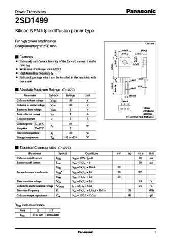
Power Transistors 2SD1499 Silicon NPN triple diffusion planar type For high power amplification Unit mm Complementary to 2SB1063 10.0 0.2 4.2 0.2 5.5 0.2 2.7 0.2 Features Extremely satisfactory linearity of the forward current transfer 3.1 0.1 ratio hFE Wide area of safe operation (ASO) High transition frequency fT Full-pack package which can be installed to the heat... See More ⇒
9.6. Size:187K lge
2sd1499.pdf 

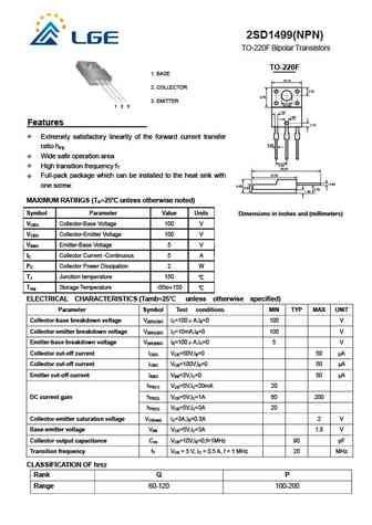
2SD1499(NPN) TO-220F Bipolar Transistors TO-220F 1. BASE 2. COLLECTOR 3. EMITTER 1 2 3 Features Extremely satisfactory linearity of the forward current transfer ratio hFE Wide safe operation area High transition frequency fT Full-pack package which can be installed to the heat sink with one screw. MAXIMUM RATINGS (TA=25 unless otherwise noted) Symbol Parameter ... See More ⇒
9.7. Size:215K inchange semiconductor
2sd1499.pdf 
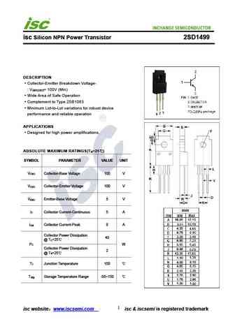
isc Silicon NPN Power Transistor 2SD1499 DESCRIPTION Collector-Emitter Breakdown Voltage- V = 100V (Min) (BR)CEO Wide Area of Safe Operation Complement to Type 2SB1063 Minimum Lot-to-Lot variations for robust device performance and reliable operation APPLICATIONS Designed for high power amplifications. ABSOLUTE MAXIMUM RATINGS(T =25 ) a SYMBOL PARAMETER VALUE UNIT V ... See More ⇒
9.8. Size:211K inchange semiconductor
2sd1494.pdf 
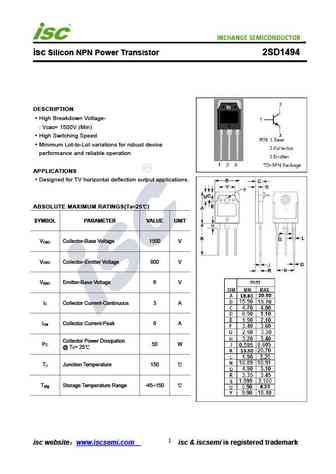
isc Silicon NPN Power Transistor 2SD1494 DESCRIPTION High Breakdown Voltage- V = 1500V (Min) CBO High Switching Speed Minimum Lot-to-Lot variations for robust device performance and reliable operation APPLICATIONS Designed for TV horizontal deflection output applications. ABSOLUTE MAXIMUM RATINGS(T =25 ) a SYMBOL PARAMETER VALUE UNIT V Collector-Base Voltage 1500 V CBO... See More ⇒
9.9. Size:186K inchange semiconductor
2sd1492.pdf 
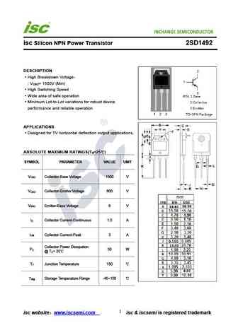
INCHANGE Semiconductor isc Silicon NPN Power Transistor 2SD1492 DESCRIPTION High Breakdown Voltage- V = 1500V (Min) CBO High Switching Speed Wide area of safe operation Minimum Lot-to-Lot variations for robust device performance and reliable operation APPLICATIONS Designed for TV horizontal deflection output applications. ABSOLUTE MAXIMUM RATINGS(T =25 ) a SYMBOL PAR... See More ⇒
9.10. Size:211K inchange semiconductor
2sd1496.pdf 
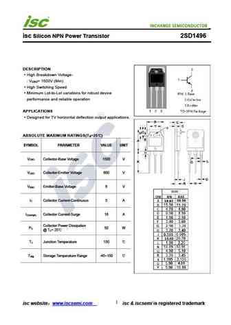
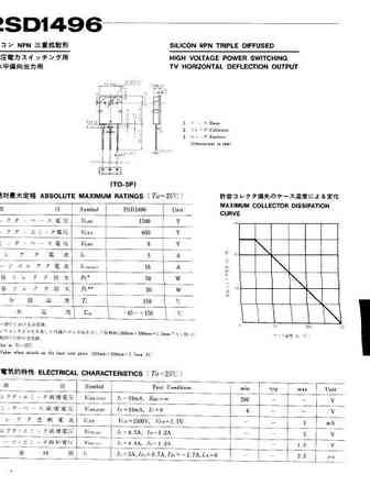
isc Silicon NPN Power Transistor 2SD1496 DESCRIPTION High Breakdown Voltage- V = 1500V (Min) CBO High Switching Speed Minimum Lot-to-Lot variations for robust device performance and reliable operation APPLICATIONS Designed for TV horizontal deflection output applications. ABSOLUTE MAXIMUM RATINGS(T =25 ) a SYMBOL PARAMETER VALUE UNIT V Collector-Base Voltage 1500 V CBO... See More ⇒
9.11. Size:212K inchange semiconductor
2sd1497.pdf 
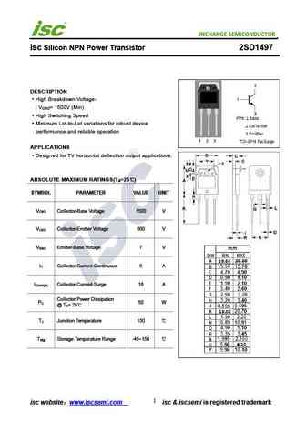
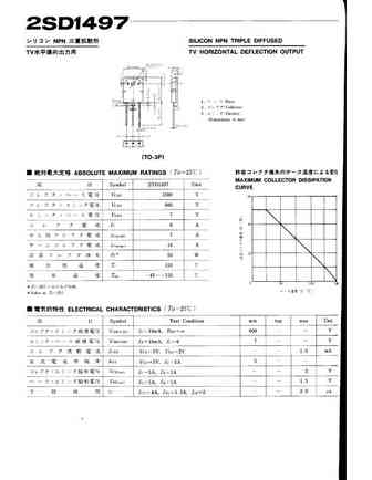
isc Silicon NPN Power Transistor 2SD1497 DESCRIPTION High Breakdown Voltage- V = 1500V (Min) CBO High Switching Speed Minimum Lot-to-Lot variations for robust device performance and reliable operation APPLICATIONS Designed for TV horizontal deflection output applications. ABSOLUTE MAXIMUM RATINGS(T =25 ) a SYMBOL PARAMETER VALUE UNIT V Collector-Base Voltage 1500 V CBO... See More ⇒
9.12. Size:210K inchange semiconductor
2sd1493.pdf 
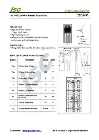
isc Silicon NPN Power Transistor 2SD1493 DESCRIPTION High Breakdown Voltage- V = 1500V (Min) CBO High Switching Speed Minimum Lot-to-Lot variations for robust device performance and reliable operation APPLICATIONS Designed for TV horizontal deflection output applications. ABSOLUTE MAXIMUM RATINGS(T =25 ) a SYMBOL PARAMETER VALUE UNIT V Collector-Base Voltage 1500 V CBO... See More ⇒
9.13. Size:210K inchange semiconductor
2sd1495.pdf 
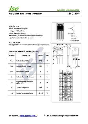
isc Silicon NPN Power Transistor 2SD1495 DESCRIPTION High Breakdown Voltage- V = 1500V (Min) CBO High Switching Speed Minimum Lot-to-Lot variations for robust device performance and reliable operation APPLICATIONS Designed for TV horizontal deflection output applications. ABSOLUTE MAXIMUM RATINGS(T =25 ) a SYMBOL PARAMETER VALUE UNIT V Collector-Base Voltage 1500 V CBO... See More ⇒
Detailed specifications: SD1455, SD1458, SD1459, SD1460, SD1462, SD1480, SD1487, SD1489, 2SD313, SD1536-03, SD1540, SD1726, SD1728, SD1729, SD1730, SD1733, MPS2222AG
Keywords - SD1490 pdf specs
SD1490 cross reference
SD1490 equivalent finder
SD1490 pdf lookup
SD1490 substitution
SD1490 replacement
