MJE271G Datasheet. Specs and Replacement
Type Designator: MJE271G 📄📄
SMD Transistor Code: JE271
Material of Transistor: Si
Polarity: PNP
Absolute Maximum Ratings
Maximum Collector Power Dissipation (Pc): 15 W
Maximum Collector-Base Voltage |Vcb|: 100 V
Maximum Collector-Emitter Voltage |Vce|: 100 V
Maximum Emitter-Base Voltage |Veb|: 5 V
Maximum Collector Current |Ic max|: 2 A
Max. Operating Junction Temperature (Tj): 150 °C
Electrical Characteristics
Transition Frequency (ft): 6 MHz
Forward Current Transfer Ratio (hFE), MIN: 500
Package: TO126
MJE271G Substitution
- BJT ⓘ Cross-Reference Search
MJE271G datasheet
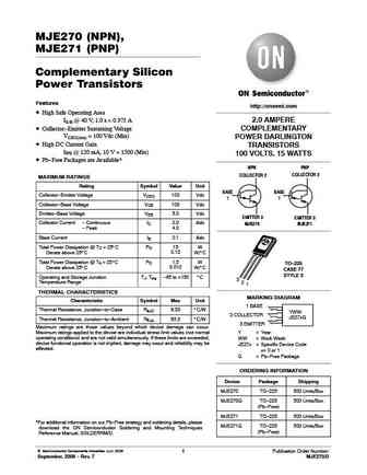
MJE270 (NPN), MJE271 (PNP) Complementary Silicon Power Transistors Features http //onsemi.com High Safe Operating Area IS/B @ 40 V, 1.0 s = 0.375 A 2.0 AMPERE Collector-Emitter Sustaining Voltage COMPLEMENTARY VCEO(sus) = 100 Vdc (Min) POWER DARLINGTON High DC Current Gain TRANSISTORS hFE @ 120 mA, 10 V = 1500 (Min) 100 VOLTS, 15 WATTS Pb-Free Packages are Availab... See More ⇒
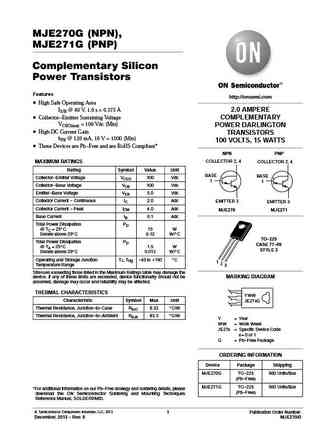
MJE270G (NPN), MJE271G (PNP) Complementary Silicon Power Transistors Features http //onsemi.com High Safe Operating Area IS/B @ 40 V, 1.0 s = 0.375 A 2.0 AMPERE Collector-Emitter Sustaining Voltage COMPLEMENTARY VCEO(sus) = 100 Vdc (Min) POWER DARLINGTON High DC Current Gain TRANSISTORS hFE @ 120 mA, 10 V = 1500 (Min) 100 VOLTS, 15 WATTS These Devices are Pb-Free ... See More ⇒
MJE270 (NPN), MJE271 (PNP) Complementary Silicon Power Transistors Features http //onsemi.com High Safe Operating Area IS/B @ 40 V, 1.0 s = 0.375 A 2.0 AMPERE Collector-Emitter Sustaining Voltage COMPLEMENTARY VCEO(sus) = 100 Vdc (Min) POWER DARLINGTON High DC Current Gain TRANSISTORS hFE @ 120 mA, 10 V = 1500 (Min) 100 VOLTS, 15 WATTS Pb-Free Packages are Availab... See More ⇒
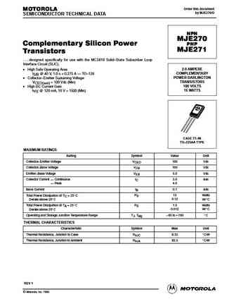
Order this document MOTOROLA by MJE270/D SEMICONDUCTOR TECHNICAL DATA NPN MJE270 Complementary Silicon Power PNP MJE271 Transistors . . . designed specifically for use with the MC3419 Solid State Subscriber Loop Interface Circuit (SLIC). High Safe Operating Area 2.0 AMPERE IS/B @ 40 V, 1.0 s = 0.375 A TO 126 COMPLEMENTARY Collector Emitter Sustaining Voltage POWE... See More ⇒
Detailed specifications: MJE181G, MJE182G, MJE200G, MJE210G, MJE210T, MJE243G, MJE253G, MJE270G, A1013, MJE2955A, MJE2955TG, MJE3055A, MJE3055TG, MJE340G, MJE3439G, MJE344G, MJE371G
Keywords - MJE271G pdf specs
MJE271G cross reference
MJE271G equivalent finder
MJE271G pdf lookup
MJE271G substitution
MJE271G replacement
History: MJE13007G | MJE13005P7 | 2SC3891A | MJE3055A | 2SD915 | MJE13005Q7
🌐 : EN ES РУ
LIST
Last Update
BJT: GA1A4M | SBT42 | 2SA200-Y | 2SA200-O | 2SD882-Q | 2SD882-P
Popular searches
2n4401 | bc547 transistor | bd139 | 2n4401 datasheet | irf640 | irf840 | irf740 | c945 transistor


