2N91 Datasheet. Specs and Replacement
Type Designator: 2N91
Material of Transistor: Ge
Polarity: PNP
Absolute Maximum Ratings
Maximum Collector Power Dissipation (Pc): 0.125 W
Maximum Collector-Base Voltage |Vcb|: 15 V
Maximum Collector Current |Ic max|: 0.5 A
Max. Operating Junction Temperature (Tj): 75 °C
Electrical Characteristics
Collector Capacitance (Cc): 75 pF
Forward Current Transfer Ratio (hFE), MIN: 15
Package: TO22
2N91 Substitution
- BJT ⓘ Cross-Reference Search
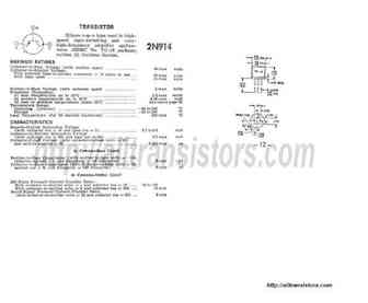
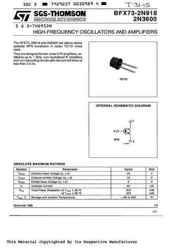
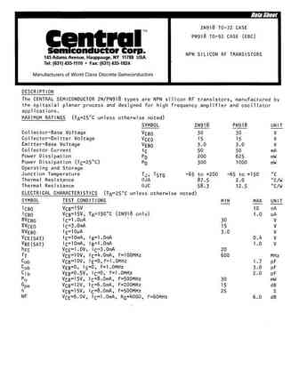
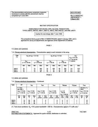
2N91 datasheet
This Material Copyrighted By Its Respective Manufacturer This Material Copyrighted By Its Respective Manufacturer This Material Copyrighted By Its Respective Manufacturer This Material Copyrighted By Its Respective Manufacturer This Material Copyrighted By Its Respective Manufacturer ... See More ⇒
145 Adams Avenue, Hauppauge, NY 11788 USA Tel (631) 435-1110 Fax (631) 435-1824 ... See More ⇒
The documentation and process conversion measures INCH-POUND necessary to comply with this amendment shall be completed by 6 June 2001. MIL-S-19500/274C AMENDMENT 1 6 March 2001 MILITARY SPECIFICATION SEMICONDUCTOR DEVICE, NPN, SILICON, TRANSISTORS TYPES 2N910, 2N910S, 2N911, 2N911S, 2N912, AND 2N912S, JAN AND JANTX Inactive for new design after 7 June 1999. This amendment forms a par... See More ⇒
Detailed specifications: 2N902, 2N903, 2N904, 2N905, 2N906, 2N907, 2N908, 2N909, A42, 2N910, 2N911, 2N912, 2N913, 2N914, 2N914-46, 2N914-51, 2N914A
Keywords - 2N91 pdf specs
2N91 cross reference
2N91 equivalent finder
2N91 pdf lookup
2N91 substitution
2N91 replacement
History: FN4L4M | STN2222A | STN2907 | DRC9144G | DMG26402 | STN2222AS | BC817-16LT1G
🌐 : EN ES РУ
LIST
Last Update
BJT: GA1A4M | SBT42 | 2SA200-Y | 2SA200-O | 2SD882-Q | 2SD882-P
Popular searches
2sc1815 replacement | 2sc2383 | c3198 transistor | irfb3607pbf datasheet | 60n60 | 2n5485 equivalent | 2sa1941 | 2sc485
