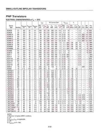
BCX17CSM Datasheet. Specs and Replacement
Type Designator: BCX17CSM 📄📄
Material of Transistor: Si
Polarity: PNP
Absolute Maximum Ratings
Maximum Collector Power Dissipation (Pc): 0.35 W
Maximum Collector-Base Voltage |Vcb|: 50 V
Maximum Collector-Emitter Voltage |Vce|: 45 V
Maximum Emitter-Base Voltage |Veb|: 5 V
Maximum Collector Current |Ic max|: 0.5 A
Max. Operating Junction Temperature (Tj): 200 °C
Electrical Characteristics
Transition Frequency (ft): 100 MHz
Collector Capacitance (Cc): 8 pF
Forward Current Transfer Ratio (hFE), MIN: 100
Noise Figure, dB: -
Package: LCC1
📄📄 Copy
- BJT ⓘ Cross-Reference Search
BCX17CSM datasheet
..1. Size:16K semelab
bcx17csm.pdf 

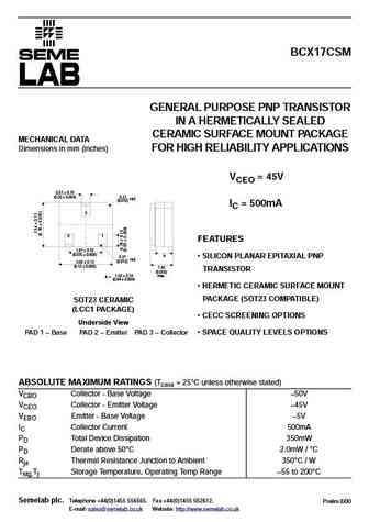
BCX17CSM GENERAL PURPOSE PNP TRANSISTOR IN A HERMETICALLY SEALED CERAMIC SURFACE MOUNT PACKAGE MECHANICAL DATA Dimensions in mm (inches) FOR HIGH RELIABILITY APPLICATIONS VCEO = 45V 0.51 0.10 (0.02 0.004) 0.31 rad. (0.012) IC = 500mA 3 21 FEATURES 1.91 0.10 (0.075 0.004) A SILICON PLANAR EPITAXIAL PNP 0.31 rad. (0.012) 3.05 0.13 (0.12 0.005) 1.40 ... See More ⇒
9.1. Size:87K motorola
bcx17lt1 bcx18lt1 bcx19lt1 bcx20lt1.pdf 

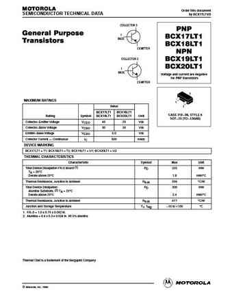
MOTOROLA Order this document SEMICONDUCTOR TECHNICAL DATA by BCX17LT1/D COLLECTOR 3 PNP General Purpose 1 BCX17LT1 BASE Transistors BCX18LT1 2 EMITTER NPN COLLECTOR 3 BCX19LT1 BCX20LT1 1 BASE Voltage and current are negative for PNP transistors 2 EMITTER 3 MAXIMUM RATINGS 1 Value 2 BCX17LT1 BCX18LT1 CASE 318 08, STYLE 6 Rating Symbol BCX19LT1 BCX20LT1 Unit SOT ... See More ⇒
9.2. Size:47K philips
bcx17 bcx18 3.pdf 

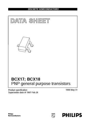
DISCRETE SEMICONDUCTORS DATA SHEET ook, halfpage M3D088 BCX17; BCX18 PNP general purpose transistors 1999 May 31 Product specification Supersedes data of 1997 Feb 28 Philips Semiconductors Product specification PNP general purpose transistors BCX17; BCX18 FEATURES PINNING High current (max. 500 mA) PIN DESCRIPTION Low voltage (max. 45 V). 1 base 2 emitter APPLICATIONS ... See More ⇒
9.3. Size:107K philips
bcx17 bcx18.pdf 

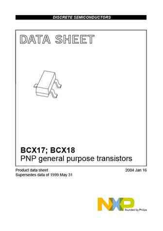
DISCRETE SEMICONDUCTORS DATA SHEET BCX17; BCX18 PNP general purpose transistors Product data sheet 2004 Jan 16 Supersedes data of 1999 May 31 NXP Semiconductors Product data sheet PNP general purpose transistors BCX17; BCX18 FEATURES PINNING High current (max. 500 mA) PIN DESCRIPTION Low voltage (max. 45 V). 1 base 2 emitter APPLICATIONS 3 collector Saturated swi... See More ⇒
9.4. Size:56K st
bcx17.pdf 

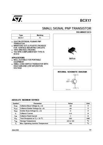
BCX17 SMALL SIGNAL PNP TRANSISTOR PRELIMINARY DATA Type Marking BCX17 T1 SILICON EPITAXIAL PLANAR PNP TRANSISTOR MINIATURE SOT-23 PLASTIC PACKAGE FOR SURFACE MOUNTING CIRCUITS TAPE AND REEL PACKING THE NPN COMPLEMENTARY TYPE IS BCX19 APPLICATIONS SOT-23 WELL SUITABLE FOR PORTABLE EQUIPMENT SMALL LOAD SWITCH TRANSISTOR WITH HIGH GAIN AND LOW SATURATION VOLTAGE INTER... See More ⇒
9.5. Size:44K fairchild semi
bcx17.pdf 

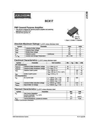
BCX17 PNP General Purpose Amplifier 3 This device is esigned for general purpose amplifier and switching application at current 0.5A. Sourced from process 78. 2 SOT-23 1 Mark T1 1. Base 2. Emitter 3. Collector Absolute Maximum Ratings TC=25 C unless otherwise noted Symbol Parameter Value Units VCEO Collector-Emitter Voltage 45 V VCBO Collector-Base Voltage 50 V VEBO E... See More ⇒
9.6. Size:297K nxp
bcx17 bcx18.pdf 

Important notice Dear Customer, On 7 February 2017 the former NXP Standard Product business became a new company with the tradename Nexperia. Nexperia is an industry leading supplier of Discrete, Logic and PowerMOS semiconductors with its focus on the automotive, industrial, computing, consumer and wearable application markets In data sheets and application notes which still contain... See More ⇒
9.7. Size:135K rohm
bcx17.pdf 

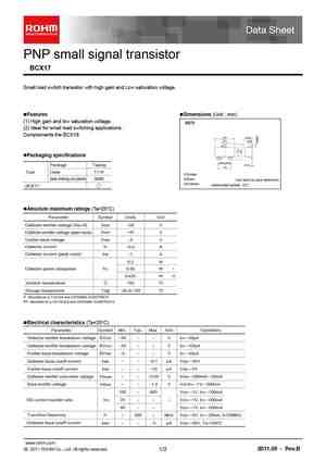
PNP small signal transistor BCX17 Small load switch transistor with high gain and Low saturation voltage. Features Dimensions (Unit mm) (1) High gain and low saturation voltage. SST3 (2) Ideal for small load switching applications. Complements the BCX19 2.9 0.95 0.4 0.45 (3) Packaging specifications (2) (1) 0.95 0.95 0.15 Package Taping 1.9 Type Code T116 (... See More ⇒
9.8. Size:99K onsemi
bcx17lt1g bcx18lt1g bcx19lt1g.pdf 

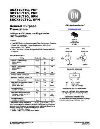
BCX17LT1G, PNP BCX18LT1G, PNP BCX19LT1G, NPN SBCX19LT1G, NPN General Purpose www.onsemi.com Transistors Voltage and Current are Negative for PNP Transistors SOT-23 Features (TO-236) CASE 318-08 S and NSV Prefix for Automotive and Other Applications Requiring STYLE 6 Unique Site and Control Change Requirements; AEC-Q101 Qualified and PPAP Capable PNP NPN These Devices a... See More ⇒
9.9. Size:61K onsemi
nsvbcx17lt1g.pdf 

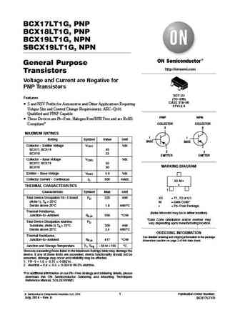
BCX17LT1G, PNP BCX18LT1G, PNP BCX19LT1G, NPN SBCX19LT1G, NPN General Purpose http //onsemi.com Transistors Voltage and Current are Negative for PNP Transistors SOT-23 Features (TO-236) CASE 318-08 S and NSV Prefix for Automotive and Other Applications Requiring STYLE 6 Unique Site and Control Change Requirements; AEC-Q101 Qualified and PPAP Capable PNP NPN These Device... See More ⇒
9.10. Size:102K onsemi
bcx17lt1g.pdf 

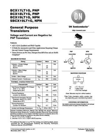
BCX17LT1G, PNP BCX18LT1G, PNP BCX19LT1G, NPN SBCX19LT1G, NPN General Purpose http //onsemi.com Transistors Voltage and Current are Negative for PNP Transistors SOT-23 Features (TO-236) CASE 318-08 AEC-Q101 Qualified and PPAP Capable STYLE 6 S Prefix for Automotive and Other Applications Requiring Unique Site and Control Change Requirements PNP NPN These Devices are... See More ⇒
9.11. Size:139K cdil
bcx17 bcx18.pdf 

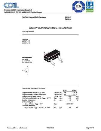
Continental Device India Limited An ISO/TS 16949, ISO 9001 and ISO 14001 Certified Company SOT-23 Formed SMD Package BCX17 BCX18 SILICON PLANAR EPITAXIAL TRANSISTORS P N P transistors Marking BCX17 = T1 BCX18 = T2 Pin configuration 1 = BASE 2 = EMITTER 3 = COLLECTOR 3 1 2 ABSOLUTE MAXIMUM RATINGS BCX17 BCX18 Collector emitter voltage (VBE = 0) VCES max. 50 30 V Colle... See More ⇒
Detailed specifications: BCW35X, BCW65ALT1G, BCW65CLT1G, BCW66GLT1G, BCW68GLT1G, BCW70LT1G, BCW72LT1G, BCX13, MJE350, BCX17LT1G, BCX19LT1G, BCX5616Q, BCY38A, BCY39A, BCY40A, BCY54A, BCY59DCSM
Keywords - BCX17CSM pdf specs
BCX17CSM cross reference
BCX17CSM equivalent finder
BCX17CSM pdf lookup
BCX17CSM substitution
BCX17CSM replacement
![]()
