DD04 Specs and Replacement
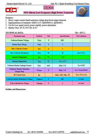
Type Designator: DD04
Material of Transistor: Si
Polarity: NPN
Absolute Maximum Ratings
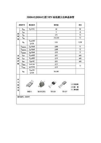
Maximum Collector Power Dissipation (Pc): 30 W
Maximum Collector-Emitter Voltage |Vce|: 160 V
Maximum Emitter-Base Voltage |Veb|: 5 V
Maximum Collector Current |Ic max|: 3 A
Max. Operating Junction Temperature (Tj): 175 °C
Electrical Characteristics
Forward Current Transfer Ratio (hFE), MIN: 50
Noise Figure, dB: -
Package: TO-3
- BJT ⓘ Cross-Reference Search
DD04 datasheet
..1. Size:23K shaanxi
dd04.pdf 

Shaanxi Qunli Electric Co., Ltd Add. No. 1 Qunli Road,Baoji City,Shaanxi,China DD04 NPN Silicon Low Frequency High Power Transistor Features 1. Heavy output current.Small saturation voltage drop.Good output character. 2. Implementation of standards GJB33 A-97, QZJ840611A, QZJ840611 3. Use for Low-speed switch, power amplify, power adjustment. 4. Quality Class JP, JT, JCT, GS, G,... See More ⇒
0.1. Size:291K 1
ndf04n60z ndd04n60z.pdf 

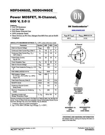
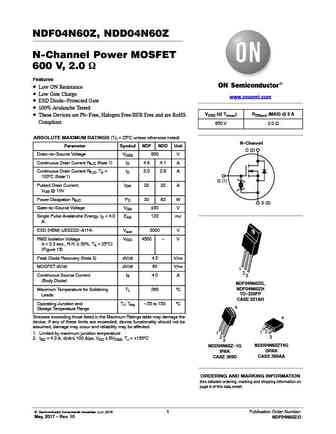
NDF04N60Z, NDD04N60Z Power MOSFET, N-Channel, 600 V, 2.0 W Features Low ON Resistance Low Gate Charge www.onsemi.com ESD Diode-Protected Gate 100% Avalanche Tested VDSS (@ TJmax) RDS(on) (MAX) @ 2 A These Devices are Pb-Free, Halogen Free/BFR Free and are RoHS Compliant 650 V 2.0 ABSOLUTE MAXIMUM RATINGS (TC = 25 C unless otherwise noted) N-Channel Param... See More ⇒
0.2. Size:148K 1
ndf04n60z ndp04n60z ndd04n60z.pdf 

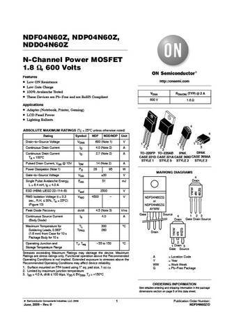
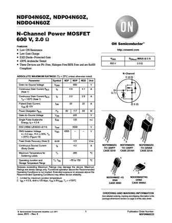
NDF04N60Z, NDP04N60Z, NDD04N60Z N-Channel Power MOSFET 1.8 W, 600 Volts Features http //onsemi.com Low ON Resistance Low Gate Charge 100% Avalanche Tested VDSS RDS(ON) (TYP) @ 2 A These Devices are Pb-Free and are RoHS Compliant 600 V 1.8 Applications Adapter (Notebook, Printer, Gaming) LCD Panel Power Lighting Ballasts 4 ABSOLUTE MAXIMUM RATINGS... See More ⇒
0.3. Size:290K fairchild semi
fdd044an03l fdu044an03l.pdf 

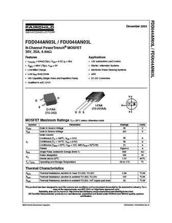
December 2003 FDD044AN03L / FDU044AN03L N-Channel PowerTrench MOSFET 30V, 35A, 4.4m Features Applications rDS(ON) = 3.6m (Typ.), VGS = 4.5V, ID = 35A 12V Automotive Load Control Qg(5) = 48nC (Typ.), VGS = 5V Starter / Alternator Systems Low Miller Charge Electronic Power Steering Systems Low QRR Body Diode ABS UIS Capability (Single Pulse and... See More ⇒
0.4. Size:118K onsemi
ndd04n50z.pdf 

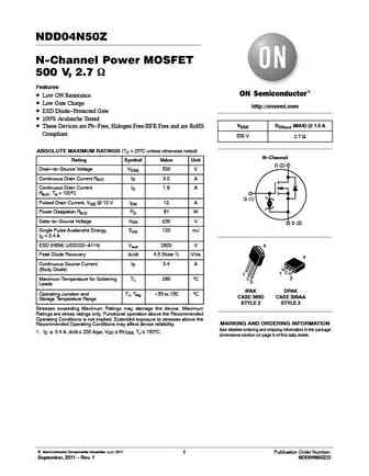
NDD04N50Z N-Channel Power MOSFET 500 V, 2.7 W Features Low ON Resistance Low Gate Charge http //onsemi.com ESD Diode-Protected Gate 100% Avalanche Tested VDSS RDS(on) (MAX) @ 1.5 A These Devices are Pb-Free, Halogen Free/BFR Free and are RoHS Compliant 500 V 2.7 W ABSOLUTE MAXIMUM RATINGS (TC = 25 C unless otherwise noted) N-Channel Rating Symbol Value Unit ... See More ⇒
0.5. Size:136K onsemi
ndf04n60z ndd04n60z.pdf 

NDF04N60Z, NDD04N60Z N-Channel Power MOSFET 600 V, 2.0 W Features Low ON Resistance Low Gate Charge www.onsemi.com ESD Diode-Protected Gate 100% Avalanche Tested VDSS (@ TJmax) RDS(on) (MAX) @ 2 A These Devices are Pb-Free, Halogen Free/BFR Free and are RoHS Compliant 650 V 2.0 ABSOLUTE MAXIMUM RATINGS (TC = 25 C unless otherwise noted) N-Channel Paramete... See More ⇒
0.6. Size:130K onsemi
ndf04n60z ndp04n60z ndd04n60z.pdf 

NDF04N60Z, NDP04N60Z, NDD04N60Z N-Channel Power MOSFET 600 V, 2.0 W Features http //onsemi.com Low ON Resistance Low Gate Charge ESD Diode-Protected Gate VDSS RDS(on) (MAX) @ 2 A 100% Avalanche Tested 600 V 2.0 These Devices are Pb-Free, Halogen Free/BFR Free and are RoHS Compliant N-Channel ABSOLUTE MAXIMUM RATINGS (TC = 25 C unless otherwise noted) D (... See More ⇒
0.7. Size:152K onsemi
ndf04n62z ndd04n62z.pdf 

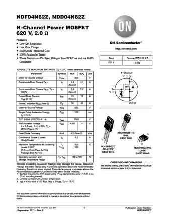
NDF04N62Z, NDD04N62Z N-Channel Power MOSFET 620 V, 2.0 W Features Low ON Resistance Low Gate Charge http //onsemi.com ESD Diode-Protected Gate 100% Avalanche Tested VDSS RDS(ON) (MAX) @ 2 A These Devices are Pb-Free, Halogen Free/BFR Free and are RoHS Compliant 620 V 2.0 W ABSOLUTE MAXIMUM RATINGS (TC = 25 C unless otherwise noted) N-Channel Parameter Symbol... See More ⇒
0.8. Size:128K samhop
sdu04n65 sdd04n65.pdf 

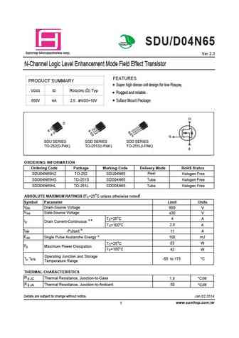
Green SDU/D04N65 Product SamHop Microelectronics corp. Ver 2.3 N-Channel Logic Level Enhancement Mode Field Effect Transistor FEATURES PRODUCT SUMMARY Super high dense cell design for low RDS(ON). VDSS ID RDS(ON) ( ) Typ Rugged and reliable. 650V 4A 2.5 @VGS=10V Suface Mount Package. D G S SDU SERIES SDD SERIES SDD SERIES TO-252(D-PAK) TO-251S(I-PAK) TO-251L(I-PAK) ORDERING IN... See More ⇒
0.9. Size:155K samhop
sdu04n60 sdd04n60.pdf 

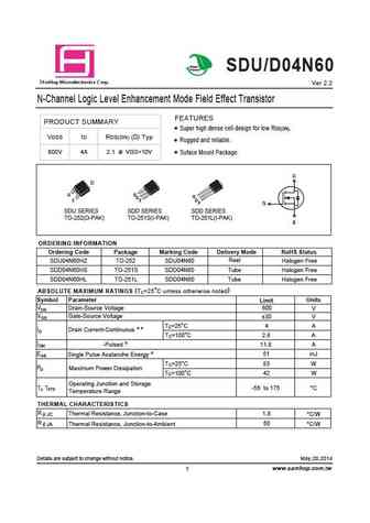
Green Product SDU/D04N60 a S mHop Microelectronics C orp. Ver 2.2 N-Channel Logic Level Enhancement Mode Field Effect Transistor FEATURES PRODUCT SUMMARY Super high dense cell design for low RDS(ON). VDSS ID RDS(ON) ( ) Typ Rugged and reliable. 600V 4A 2.1 @ VGS=10V Suface Mount Package. D G S SDU SERIES SDD SERIES SDD SERIES TO-252(D-PAK) TO-251S(I-PAK) TO-251L(I-PAK) ORDERIN... See More ⇒
0.12. Size:327K inchange semiconductor
ndd04n60z-1g.pdf 
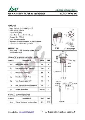
isc N-Channel MOSFET Transistor NDD04N60Z-1G FEATURES Drain Current I = 4.5A@ T =25 D C Drain Source Voltage V = 650V(Min) DSS Static Drain-Source On-Resistance R = 2.1 (Max) DS(on) 100% avalanche tested Minimum Lot-to-Lot variations for robust device performance and reliable operation DESCRIPTION motor drive, DC-DC converter, power switch and solenoid drive... See More ⇒
0.13. Size:309K inchange semiconductor
fdd044an03l.pdf 
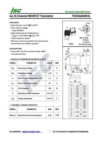
isc N-Channel MOSFET Transistor FDD044AN03L FEATURES Drain Current I =21A@ T =25 D C Drain Source Voltage V =30V(Min) DSS Static Drain-Source On-Resistance R =3.9m (Max) @ V = 10V DS(on) GS 100% avalanche tested Minimum Lot-to-Lot variations for robust device performance and reliable operation DESCRIPTION motor drive, DC-DC converter, power switch and soleno... See More ⇒
Detailed specifications: CHUMF22GP, CHUMF23GP, CHUMF24GP, CHUMF4GP, CHUMF5GP, CHUMF7GP, CHUMF8GP, DD03T, 2N4401, DD04T, DD05, DD05T, DMA50101, DMA50201, DMA50401, DMA50601, DMA50601
Keywords - DD04 pdf specs
DD04 cross reference
DD04 equivalent finder
DD04 pdf lookup
DD04 substitution
DD04 replacement
![]()
