MMDT5551DW Specs and Replacement
Type Designator: MMDT5551DW
SMD Transistor Code: G1
Material of Transistor: Si
Polarity: NPN
Absolute Maximum Ratings
Maximum Collector Power Dissipation (Pc): 0.2 W
Maximum Collector-Base Voltage |Vcb|: 180 V
Maximum Collector-Emitter Voltage |Vce|: 160 V
Maximum Emitter-Base Voltage |Veb|: 6 V
Maximum Collector Current |Ic max|: 0.2 A
Max. Operating Junction Temperature (Tj): 150 °C
Electrical Characteristics
Transition Frequency (ft): 100 MHz
Collector Capacitance (Cc): 6 pF
Forward Current Transfer Ratio (hFE), MIN: 100
Package: SOT363
MMDT5551DW Substitution
- BJT ⓘ Cross-Reference Search
MMDT5551DW datasheet
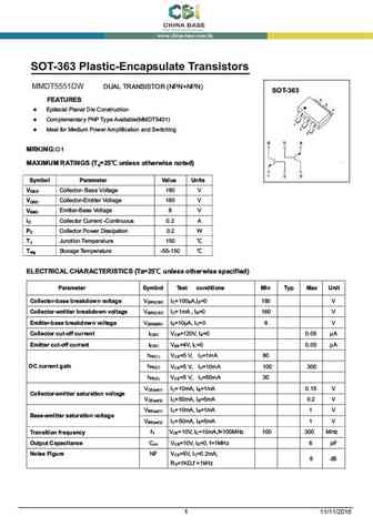
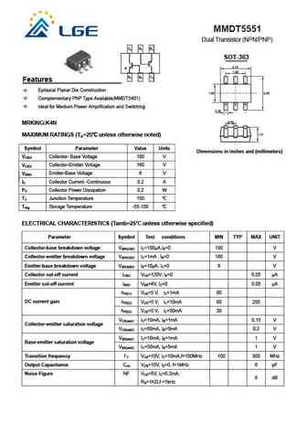
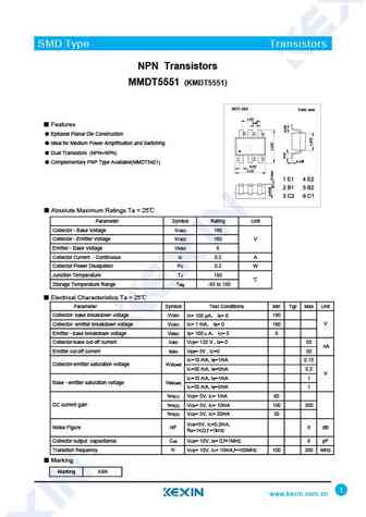
MMDT5551DW DUAL TRANSISTOR (NPN+NPN) 6 5 4 Epitaxial Planar Die Construction Complementary PNP Type Available(MMDT5401) 1 2 Ideal for Medium Power Amplification and Switching 3 G1 ... See More ⇒
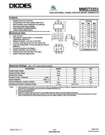
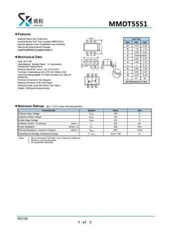
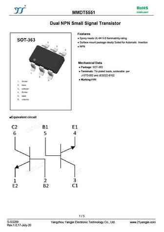
MMDT5551 DUAL NPN SMALL SIGNAL SURFACE MOUNT TRANSISTOR Features A Epitaxial Planar Die Construction SOT-363 Complementary PNP Type Available (MMDT5401) C2 B1 E1 Dim Min Max Ideal for Medium Power Amplification and Switching A 0.10 0.30 B C Ultra-Small Surface Mount Package B 1.15 1.35 Lead Free/RoHS Compliant (Note 3) E2 B2 C1 C 2.00 2.20 "Gr... See More ⇒
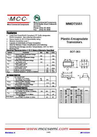
MCC TM Micro Commercial Components 20736 Marilla Street Chatsworth Micro Commercial Components MMDT5551 CA 91311 Phone (818) 701-4933 Fax (818) 701-4939 Features Lead Free Finish/RoHS Compliant ("P" Suffix designates RoHS Compliant. See ordering information) Epoxy meets UL 94 V-0 flammability rating Plastic-Encapsulate Moisure Sensitivity Level 1 Transistors C... See More ⇒
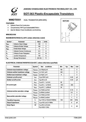
J C ET DUAL TRANSISTOR (NPN+NPN) 6 5 4 Epitaxial Planar Die Construction Complementary PNP Type Available(MMDT5401) 1 2 Ideal for Medium Power Amplification and Switching 3 ... See More ⇒
Detailed specifications: MMDT3052DW-E , MMDT3052DW-F , MMDT3052DW-G , MMDT3904DW , MMDT3906DW , MMDT3946DW , MMDT4403DW , MMDT5401DW , 2SA1943 , MMDT9014DW , FHS2222A-ME , FHS2907A-ME , FHS3904-ME , FHS3906-ME , FHT1298O-ME , FHT1298Y-ME , FHT5401-ME .
History: DDTC113TCA
Keywords - MMDT5551DW pdf specs
MMDT5551DW cross reference
MMDT5551DW equivalent finder
MMDT5551DW pdf lookup
MMDT5551DW substitution
MMDT5551DW replacement
History: DDTC113TCA
🌐 : EN ES РУ
LIST
Last Update
BJT: GA1A4M | SBT42 | 2SA200-Y
Popular searches
2sk2749 | c2577 transistor | k3563 transistor | 2sc1775 datasheet | j377 transistor datasheet | svt20240nt | tip41c replacement | b772m transistor
