View pb554dy datasheet:
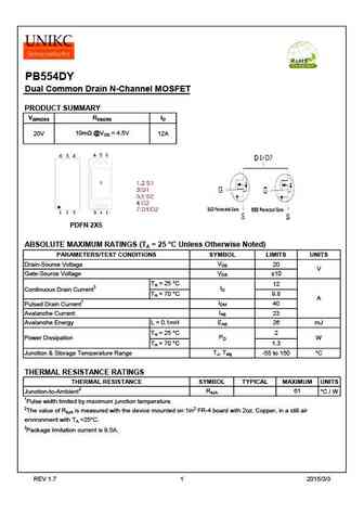
PB554DYDual Common Drain N-Channel MOSFETPRODUCT SUMMARYV(BR)DSS RDS(ON) ID10m @VGS = 4.5V20V 12APDFN 2X5ABSOLUTE MAXIMUM RATINGS (TA = 25 C Unless Otherwise Noted)PARAMETERS/TEST CONDITIONS SYMBOL LIMITS UNITSVDSDrain-Source Voltage 20VVGSGate-Source Voltage 10TA = 25 C12IDContinuous Drain Current3TA = 70 C9.8AIDM40Pulsed Drain Current1IASAvalanche Current 23EASAvalanche Energy L = 0.1mH 26 mJTA = 25 C2PDPower Dissipation WTA = 70 C1.3TJ, TstgJunction & Storage Temperature Range -55 to 150 CTHERMAL RESISTANCE RATINGSTHERMAL RESISTANCE SYMBOL TYPICAL MAXIMUM UNITSRqJA 61 C / WJunction-to-Ambient21Pulse width limited by maximum junction temperature.2The value of RqJA is measured with the device mounted on 1in2 FR-4 board with 2oz. Copper, in a still airenvironment with
Keywords - ALL TRANSISTORS DATASHEET
pb554dy.pdf Design, MOSFET, Power
pb554dy.pdf RoHS Compliant, Service, Triacs, Semiconductor
pb554dy.pdf Database, Innovation, IC, Electricity


