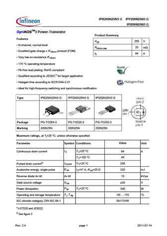
IPP200N25N3G MOSFET Equivalente. Reemplazo. Hoja de especificaciones. Principales características
Número de Parte: IPP200N25N3G
Tipo de FET: MOSFET
Polaridad de transistor: N
ESPECIFICACIONES MÁXIMAS
Pdⓘ - Máxima disipación de potencia: 300 W
|Vds|ⓘ - Voltaje máximo drenador-fuente: 250 V
|Vgs|ⓘ - Voltaje máximo fuente-puerta: 20 V
|Id|ⓘ - Corriente continua de drenaje: 64 A
Tjⓘ - Temperatura máxima de unión: 175 °C
CARACTERÍSTICAS ELÉCTRICAS
trⓘ - Tiempo de subida: 20 nS
Cossⓘ - Capacitancia de salida: 297 pF
RDSonⓘ - Resistencia estado encendido drenaje a fuente: 0.02 Ohm
Encapsulados: TO220
Búsqueda de reemplazo de IPP200N25N3G MOSFET
- Selecciónⓘ de transistores por parámetros
IPP200N25N3G datasheet
ipb200n25n3-g ipp200n25n3-g ipi200n25n3-g ipb200n25n3g ipp200n25n3g ipi200n25n3g.pdf
ipp200n25n3.pdf
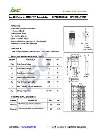
isc N-Channel MOSFET Transistor IPP200N25N3 IIPP200N25N3 FEATURES Static drain-source on-resistance RDS(on) 20m Enhancement mode Fast Switching Speed 100% avalanche tested Minimum Lot-to-Lot variations for robust device performance and reliable operation DESCRITION Ideal for high-frequency switching and synchronous rectification ABSOLUTE MAXIMUM RATINGS(T
ipb200n15n3g ipd200n15n3g ipi200n15n3g ipp200n15n3g ipb200n15n3 ipd200n15n3 ipi200n15n3 ipp200n15n3.pdf
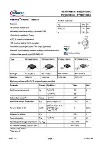
IPB200N15N3 G IPD200N15N3 G IPI200N15N3 G IPP200N15N3 G OptiMOS 3 Power-Transistor Product Summary Features VDS 150 V N-channel, normal level RDS(on),max 20 mW Excellent gate charge x R product (FOM) DS(on) ID 50 A Very low on-resistance R DS(on) 175 C operating temperature Pb-free lead plating; RoHS compliant Qualified according to JEDEC1) for t
ipp200n15n3.pdf
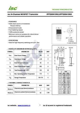
isc N-Channel MOSFET Transistor IPP200N15N3,IIPP200N15N3 FEATURES Static drain-source on-resistance RDS(on) 20m Enhancement mode Fast Switching Speed 100% avalanche tested Minimum Lot-to-Lot variations for robust device performance and reliable operation DESCRITION Ideal for high frequency switching and sync. Rec. ABSOLUTE MAXIMUM RATINGS(T =25 ) a SYMBOL
Otros transistores... IPP12CN10NG , IPP139N08N3G , IPP147N03LG , IPP147N12N3G , IPP16CN10LG , IPP16CN10NG , IPP180N10N3G , IPP200N15N3G , IRF1404 , IPP230N06L3G , IPP260N06N3G , IPP26CN10NG , IPP320N20N3G , IPP35CN10NG , IPP50CN10NG , IPP50R140CP , IPP50R199CP .
🌐 : EN ES РУ

Liste
Recientemente añadidas las descripciónes de los transistores:
MOSFET: ASB80R750E | ASB70R380E | ASB65R300E | ASB65R220E | ASB65R120EFD | ASB60R150E | ASA80R900E | ASA80R750E | ASA80R290E | ASA70R950E | ASA70R600E | ASA70R380E | ASA70R240E | ASA65R850E | ASA65R550E | ASA65R350E
Popular searches
2sc1451 datasheet | 2sc373 | a1023 datasheet | 2sc1080 | 2sb618 | 2sc1328 | 2sc1845 transistor | a933 transistor datasheet