AO3401 Datasheet. Equivalente. Reemplazo. Hoja de especificaciones. Principales características
Número de Parte: AO3401 📄📄
Tipo de FET: MOSFET
Polaridad de transistor: P
ESPECIFICACIONES MÁXIMAS
Pdⓘ - Máxima disipación de potencia: 1.4 W
|Vds|ⓘ - Voltaje máximo drenador-fuente: 30 V
|Vgs|ⓘ - Voltaje máximo fuente-puerta: 12 V
|Id|ⓘ - Corriente continua de drenaje: 4.2 A
Tjⓘ - Temperatura máxima de unión: 150 °C
CARACTERÍSTICAS ELÉCTRICAS
trⓘ - Tiempo de subida: 3.2 nS
Cossⓘ - Capacitancia de salida: 115 pF
RDSonⓘ - Resistencia estado encendido drenaje a fuente: 0.064 Ohm
Encapsulados: SOT23
📄📄 Copiar
Búsqueda de reemplazo de AO3401 MOSFET
- Selecciónⓘ de transistores por parámetros
AO3401 datasheet
..1. Size:1439K htsemi
ao3401.pdf 
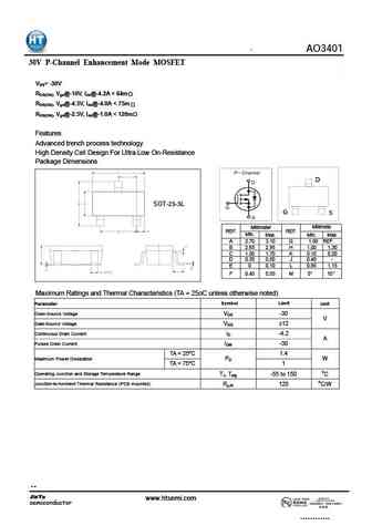
AO3401 30V P-Channel Enhancement Mode MOSFET V = -30V DS R , V DS(ON) gs@-10V, I ds@-4.2A
..2. Size:1540K lge
ao3401.pdf
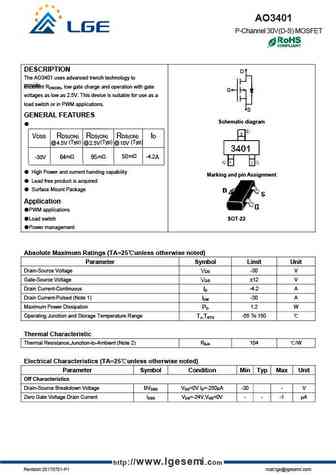
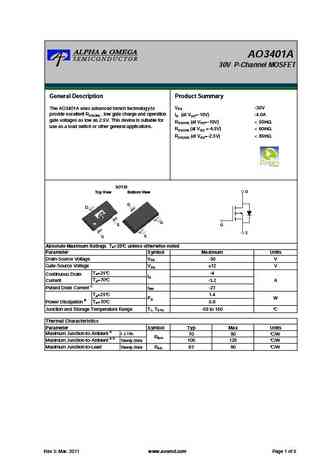
AO3401 P-Channel 30V(D-S) MOSFET DESCRIPTION D The AO3401 uses advanced trench technology to provide excellent RDS(ON), low gate charge and operation with gate G voltages as low as 2.5V. This device is suitable for use as a load switch or in PWM applications. S GENERAL FEATURES Schematic diagram VDSS RDS(ON) RDS(ON) RDS(ON) ID @ 4.5V (Typ) @ 2.5V (Typ) @ 10V (Typ)
..3. Size:497K aosemi
ao3401.pdf
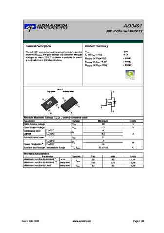
AO3401 30V P-Channel MOSFET General Description Product Summary VDS -30V The AO3401 uses advanced trench technology to provide excellent RDS(ON), low gate charge and operation with gate ID (at VGS=-10V) -4.0A voltages as low as 2.5V. This device is suitable for use as RDS(ON) (at VGS=-10V)
..4. Size:1476K shenzhen
ao3401.pdf
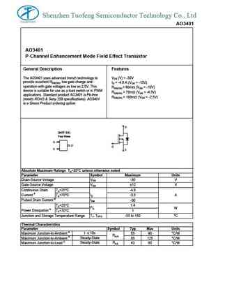
Shenzhen Tuofeng Semiconductor Technology Co., Ltd AO3401 AO3401 P-Channel Enhancement Mode Field Effect Transistor General Description Features The AO3401 uses advanced trench technology to VDS (V) = -30V provide excellent RDS(ON), low gate charge and ID = -4.0 A (VGS = -10V) operation with gate voltages as low as 2.5V. This RDS(ON)
..5. Size:771K blue-rocket-elect
ao3401.pdf
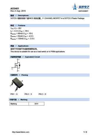
AO3401 Rev.A Aug.-2016 DATA SHEET / Descriptions SOT23-3 P MOS P- CHANNEL MOSFET in a SOT23-3 Plastic Package. / Features VDS (V) = -30V ID = -4.2 A (VGS = -10V) RDS(ON)
..6. Size:1535K kexin
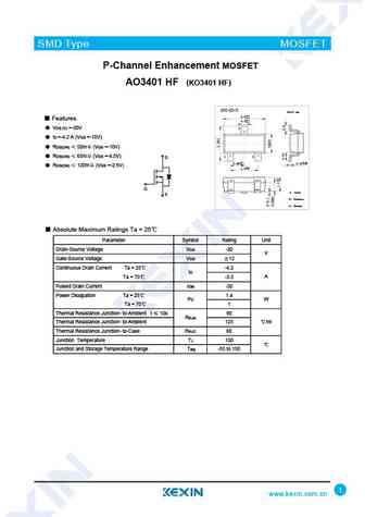
ao3401 ko3401.pdf
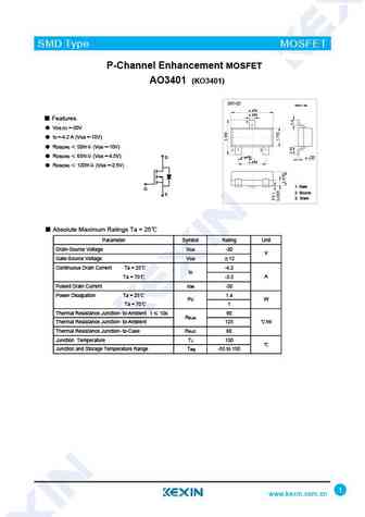
SMD Type MOSFET P-Channel Enhancement MOSFET AO3401 (KO3401) SOT-23 Unit mm 2.9+0.1 -0.1 +0.1 0.4-0.1 Features 3 VDS (V) =-30V ID =-4.2 A (VGS =-10V) RDS(ON) 50m (VGS =-10V) 1 2 +0.1 RDS(ON) 65m (VGS =-4.5V) +0.05 0.95 -0.1 0.1 -0.01 D +0.1 1.9 -0.1 RDS(ON) 120m (VGS =-2.5V) 1. Gate G 2. Source S 3. Drain Absolute M
..7. Size:1535K kexin
ao3401.pdf

SMD Type MOSFET P-Channel Enhancement MOSFET AO3401 (KO3401) SOT-23 Unit mm 2.9+0.1 -0.1 +0.1 0.4-0.1 Features 3 VDS (V) =-30V ID =-4.2 A (VGS =-10V) RDS(ON) 50m (VGS =-10V) 1 2 +0.1 RDS(ON) 65m (VGS =-4.5V) +0.05 0.95 -0.1 0.1 -0.01 D +0.1 1.9 -0.1 RDS(ON) 120m (VGS =-2.5V) 1. Gate G 2. Source S 3. Drain Absolute M
..8. Size:627K guangdong hottech
ao3401.pdf
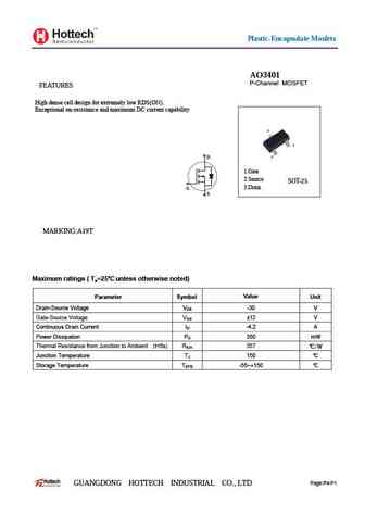
Plastic-Encapsulate Mosfets AO3401 P-Channel MOSFET FEATURES High dense cell design for extremely low RDS(ON). Exceptional on-resistance and maximum DC current capability D 1.Gate 2.Source SOT-23 3.Drain G S MARKING A19T Maximum ratings ( Ta=25 unless otherwise noted) Unit Parameter Symbol Value Drain-Source Voltage VDS -30 V Gate-Source Voltage VGS 12 V Continuous
..9. Size:1887K mdd
ao3401.pdf
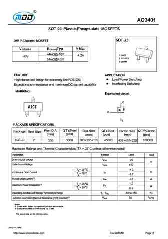
AO3401 SOT-23 Plastic-Encapsulate MOSFETS SOT-23 30V P-Channel MOSFET 3 ID Max V(BR)DSS RDS(on)Typ 44m @-10V 1. GATE -4.2A -30V 2. SOURCE 51m @4.5V 1 3. DRAIN 2 FEATURE APPLICATION Load/Power Switching High dense cell design for extremely low RDS(ON) Interfacing Switching Exceptional on-resistance and maximum DC current capability MARKING Equivalen
..10. Size:1425K cn puolop
ao3401.pdf

AO3401 -30V P-Channel Enhancement Mode MOSFET V = -30V DS R , V DS(ON) gs@-10V, I ds@-4.2A
..11. Size:453K cn shikues
ao3401.pdf
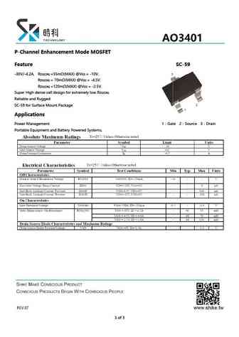
P-Channel Enhancement Mode MOSFET Channel Enhancement Mode MOSFET Feature SC-59 -30V/-4.2A, RDS(ON) =55m (MAX) @VGS = -10V. = RDS(ON) = 70m (MAX) @VGS = -4.5V. GS RDS(ON) =120m (MAX) @VGS = -2.5V. GS Super High dense cell design for extremely low R Super High dense cell design for extremely low RDS(ON) Reliable and Rugged SC-59 for Surface Mount Package Applications
..12. Size:1599K cn yongyutai
ao3401.pdf
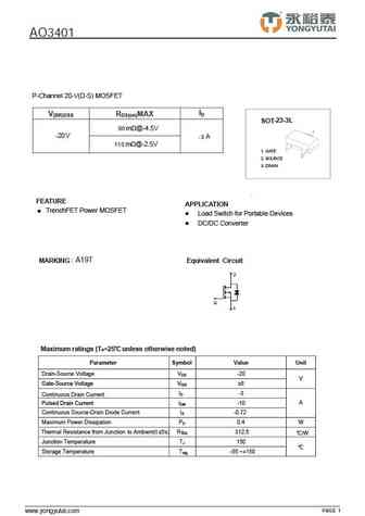
AO3401 P-Channel 20-V(D-S) MOSFET ID V(BR)DSS RDS(on)MAX SOT-23-3L 90 m @-4.5V -20V A -3 110 m @-2.5V 1. GATE 2. SOURCE 3. DRAIN FEATURE APPLICATION TrenchFET Power MOSFET z z Load Switch for Portable Devices z DC/DC Converter MARKING A19T Equivalent Circuit Maximum ratings (Ta=25 unless otherwise noted) Parameter Symbol Value Unit Drain-Source V
..13. Size:1377K cn alj
ao3401.pdf
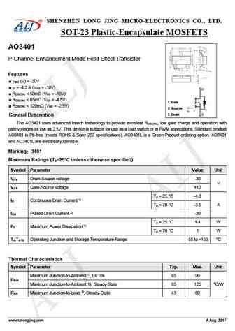
SHENZHEN LONG JING MICRO-ELECTRONICS CO., LTD. SOT-23 Plastic-Encapsulate MOSFETS AO3401 P-Channel Enhancement Mode Field Effect Transistor Features V (V) = -30V DS = -4.2 A (V = -10V) ID GS R
..14. Size:947K cn twgmc
ao3401.pdf
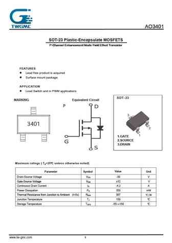
SI2305 AO3401 AO3401 AO3401 SOT-23 Plastic-Encapsulate MOSFETS FEATURES
..15. Size:867K cn vbsemi
ao3401.pdf
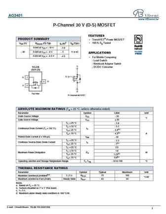
AO3401 www.VBsemi.tw P-Channel 30 V (D-S) MOSFET FEATURES PRODUCT SUMMARY TrenchFET Power MOSFET 100 % Rg Tested VDS (V) RDS(on) ( ) Typ. ID (A)a Qg (Typ.) 0.046 at VGS = - 10 V - 5.6 0.049 at VGS = - 6 V - 5 11.4 nC - 30 APPLICATIONS 0.054 at VGS = - 4.5 V -4.5 For Mobile Computing - Load Switch - Notebook Adaptor Switch S TO-236 - DC/DC Converter (SOT-23)
0.1. Size:231K aosemi
ao3401a.pdf
AO3401A 30V P-Channel MOSFET General Description Product Summary VDS -30V The AO3401A uses advanced trench technology to provide excellent RDS(ON) , low gate charge and operation ID (at VGS=-10V) -4.0A gate voltages as low as 2.5V. This device is suitable for RDS(ON) (at VGS=-10V)
0.2. Size:1580K kexin
ao3401hf.pdf
SMD Type MOSFET P-Channel Enhancement MOSFET AO3401 HF (KO3401 HF) SOT-23-3 Unit mm +0.2 2.9 -0.1 Features +0.1 0.4-0.1 VDS (V) =-30V 3 ID =-4.2 A (VGS =-10V) RDS(ON) 50m (VGS =-10V) RDS(ON) 65m (VGS =-4.5V) 1 2 D +0.02 +0.1 0.15 -0.02 0.95 -0.1 RDS(ON) 120m (VGS =-2.5V) +0.1 1.9 -0.2 G 1. Gate S 2. Source 3. Drain A
0.3. Size:1562K kexin
ao3401-3.pdf

SMD Type MOSFET P-Channel Enhancement MOSFET AO3401 (KO3401) SOT-23-3 Unit mm +0.2 2.9 -0.1 Features +0.1 0.4-0.1 VDS (V) =-30V 3 ID =-4.2 A (VGS =-10V) RDS(ON) 50m (VGS =-10V) RDS(ON) 65m (VGS =-4.5V) 1 2 D +0.02 +0.1 0.15 -0.02 0.95 -0.1 RDS(ON) 120m (VGS =-2.5V) +0.1 1.9 -0.2 G 1. Gate S 2. Source 3. Drain Absolu
0.4. Size:1315K kexin
ao3401a.pdf

SMD Type MOSFET P-Channel MOSFET AO3401A (KO3401A) SOT-23 Unit mm +0.1 2.9 -0.1 +0.1 0.4 -0.1 Features 3 VDS (V) =-30V ID =-4 A (VGS =-10V) RDS(ON) 50m (VGS =-10V) 1 2 +0.1 +0.05 0.95-0.1 0.1-0.01 RDS(ON) 60m (VGS =-4.5V) +0.1 1.9-0.1 RDS(ON) 85m (VGS =-2.5V) 1. Gate 2. Source D 3. Drain G S Absolute Maximum Ratings T
0.5. Size:1320K kexin
ao3401a-3.pdf

SMD Type MOSFET P-Channel MOSFET AO3401A (KO3401A) SOT-23-3 Unit mm +0.2 2.9 -0.1 +0.1 0.4-0.1 3 Features VDS (V) =-30V ID =-4 A (VGS =-10V) 1 2 RDS(ON) 50m (VGS =-10V) +0.02 +0.1 0.15 -0.02 0.95 -0.1 +0.1 RDS(ON) 60m (VGS =-4.5V) 1.9 -0.2 RDS(ON) 85m (VGS =-2.5V) 1. Gate 2. Source D 3. Drain G S Absolute Maximum R
0.6. Size:3338K umw-ic
ao3401a.pdf
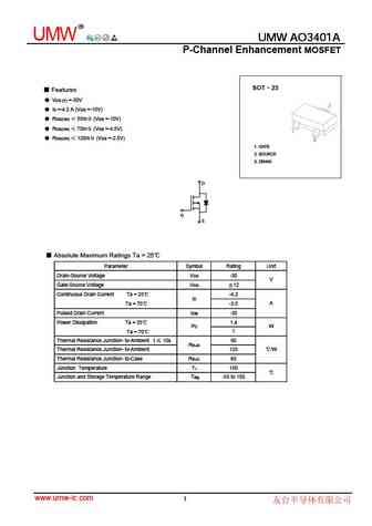
R UMWpe UMW AO3401A UMW AO3401A M SFET SMD Ty P-Channel Enhancement MOSFET SOT 23 Features VDS (V) =-30V ID =-4.2 A (VGS =-10V) RDS(ON) 55m (VGS =-10V) RDS(ON) 70m (VGS =-4.5V) RDS(ON) 120m (VGS =-2.5V) 1. GATE 2. SOURCE 3. DRAIN D G S Absolute Maximum Ratings Ta = 25 Parameter Symbol Rating Unit Drain-Source Voltage V
0.7. Size:1984K born
ao3401a.pdf
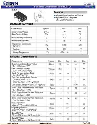
AO3401A MOSFET ROHS P-Channel Enhancement-Mode MOSFET SOT-23 - Features Advanced trench process technology High Density Cell Design For Ultra Low On-Resistance MAXIMUM RANTINGS Characteristic Symbol Max Unit -30 Drain-Source Voltage BV V DSS Gate- Source Voltage V V GS +12 Drain Current (continuous) I -4.2 A D Drain Current (pulsed) I A DM -18 Total Device D
0.8. Size:1148K born
ao3401f.pdf
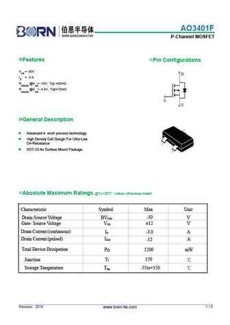
AO3401F P-Channel MOSFET Features Pin Configurations V = -30V DS I D = -3 A R @V = -10V, Typ =65m DS(ON) GS R @V = -4.5V, Typ=75m DS(ON) GS General Description Advanced tr ench process technology High Density Cell Design For Ultra Low On-Resistance SOT-23 for Surface Mount Package. Absolute Maximum Ratings @T =25 unless otherwise noted A Char
0.9. Size:468K huashuo
ao3401a.pdf
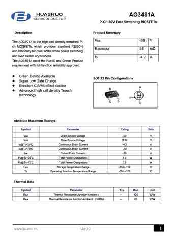
AO3401A P-Ch 30V Fast Switching MOSFETs Description Product Summary VDS -30 V The AO3401A is the high cell density trenched P- ch MOSFETs, which provides excellent RDSON RDS(ON),typ 54 m and efficiency for most of the small power switching and load switch applications. ID -4.2 A The AO3401A meet the RoHS and Green Product requirement with full function reliability approv
0.10. Size:573K msksemi
ao3401mi-ms.pdf
www.msksemi.com AO3401MI-MS Semiconductor Compiance FEATURE SOT-23-3 3 High dense cell design for extremely low R . DS(ON) Exceptional on-resistance and maximum DC currentcapability 1. GATE 1 2 APPLICATION 2. SOURCE Load/Power Switching 3. DRAIN Interfacing Switching Equivalent Circuit I V(BR)DSS RDS(on)MAX D 65m @-10V 75m @-4.5V -30 V -4.2A 90m @-2.5V
0.11. Size:866K cn vbsemi
ao3401a.pdf

AO3401A www.VBsemi.tw P-Channel 30 V (D-S) MOSFET FEATURES PRODUCT SUMMARY TrenchFET Power MOSFET 100 % Rg Tested VDS (V) RDS(on) ( ) Typ. ID (A)a Qg (Typ.) 0.046 at VGS = - 10 V - 5.6 0.049 at VGS = - 6 V - 5 11.4 nC - 30 APPLICATIONS 0.054 at VGS = - 4.5 V -4.5 For Mobile Computing - Load Switch - Notebook Adaptor Switch S TO-236 - DC/DC Converter (SOT-23)
0.12. Size:967K cn minos
ao3401s.pdf
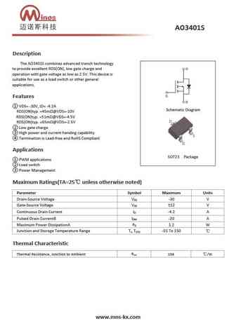
Description The AO3401S combines advanced trench technology to provide excellent RDS(ON), low gate charge and operation with gate voltage as low as 2.5V. This device is suitable for use as a load switch or other general applications. Features VDS= -30V, ID= -4.2A Schematic Diagram RDS(ON)typ. =45m @VDS=-10V RDS(ON)typ. =51m @VDS=-4.5V RDS(ON)typ. =65m @VDS=-2.5V Low gate
Otros transistores... PT8205, PT8205A, PT8822, PT4410, PT9926, SI2301, SI2305, XP152A12COMR, K4145, AO3407, PT4435, SM103, SM104, SMY50, SMY51, SMY52, SMY60
