CED02N9 MOSFET Equivalente. Reemplazo. Hoja de especificaciones. Principales características
Número de Parte: CED02N9
Tipo de FET: MOSFET
Polaridad de transistor: N
ESPECIFICACIONES MÁXIMAS
Pdⓘ - Máxima disipación de potencia: 75 W
|Vds|ⓘ - Voltaje máximo drenador-fuente: 900 V
|Vgs|ⓘ - Voltaje máximo fuente-puerta: 30 V
|Id|ⓘ - Corriente continua de drenaje: 2 A
Tjⓘ - Temperatura máxima de unión: 175 °C
CARACTERÍSTICAS ELÉCTRICAS
trⓘ - Tiempo de subida: 34 nS
Cossⓘ - Capacitancia de salida: 70 pF
RDSonⓘ - Resistencia estado encendido drenaje a fuente: 6.8 Ohm
Encapsulados: TO251
Búsqueda de reemplazo de CED02N9 MOSFET
- Selecciónⓘ de transistores por parámetros
CED02N9 datasheet
ceu02n9 ced02n9.pdf
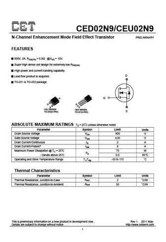
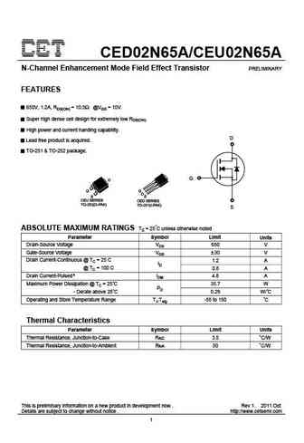
CED02N9/CEU02N9 N-Channel Enhancement Mode Field Effect Transistor PRELIMINARY FEATURES 900V, 2A, RDS(ON) = 6.8 @VGS = 10V. Super high dense cell design for extremely low RDS(ON). High power and current handing capability. D Lead free product is acquired. TO-251 & TO-252 package. D G G S CEU SERIES CED SERIES S TO-252(D-PAK) TO-251(I-PAK) ABSOLUTE MAXIMUM RATINGS Tc = 25 C u
ceu02n7g-1 ced02n7g-1.pdf
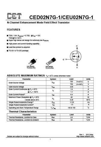
CED02N7G-1/CEU02N7G-1 N-Channel Enhancement Mode Field Effect Transistor FEATURES 720V, 1.6A, RDS(ON) = 6.75 @VGS = 10V. 750V@Tc=150 C Super high dense cell design for extremely low RDS(ON). High power and current handing capability. D Lead free product is acquired. TO-251 & TO-252 package. D G G S CEU SERIES CED SERIES S TO-252(D-PAK) TO-251(I-PAK) ABSOLUTE MAXIMUM RATING
ceu02n7g ced02n7g.pdf
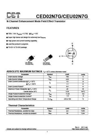
CED02N7G/CEU02N7G N-Channel Enhancement Mode Field Effect Transistor FEATURES 700V, 1.6A, RDS(ON) = 6.75 @VGS = 10V. Super high dense cell design for extremely low RDS(ON). High power and current handing capability. D Lead free product is acquired. TO-251 & TO-252 package. D G G S CEU SERIES CED SERIES S TO-252(D-PAK) TO-251(I-PAK) ABSOLUTE MAXIMUM RATINGS Tc = 25 C unless o
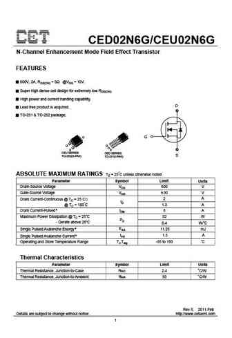
ceu02n65g ced02n65g.pdf
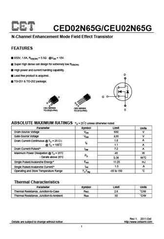
CED02N65G/CEU02N65G N-Channel Enhancement Mode Field Effect Transistor FEATURES 650V, 1.8A, RDS(ON) = 5.5 @VGS = 10V. Super high dense cell design for extremely low RDS(ON). High power and current handing capability. D Lead free product is acquired. TO-251 & TO-252 package. D G G S CEU SERIES CED SERIES S TO-252(D-PAK) TO-251(I-PAK) ABSOLUTE MAXIMUM RATINGS Tc = 25 C unless
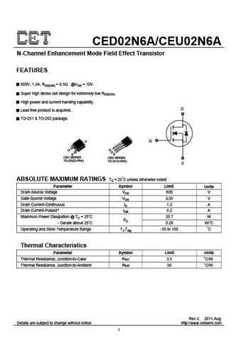
Otros transistores... CED01N6G, CED01N7, CED02N65A, CED02N65G, CED02N6A, CED02N6G, CED02N7G, CED02N7G-1, IRF640, CED03N8, CED04N6, CED04N65, CED04N7G, CED05N65, CED06N7, CED07N65A, CED08N6A
🌐 : EN ES РУ

Liste
Recientemente añadidas las descripciónes de los transistores:
MOSFET: AKF30N5P0SX | AKF30N10S | AKF20P45D | CM4407 | CM3407 | CM3400 | SVF11N65F | SVF11N65T | FKBB3105 | EHBA036R1 | CRTT067N10N | AP6NA3R2MT | AP65SA145DDT8 | AP4NAR95CMT-A | AP4024GEMT-HF | AP3P050AH
Popular searches
3sk41 | 2sc2240 transistor | c3198 | 2sc793 | 2sd313 replacement | 2n4249 | a1013 transistor | 2sc2705