CEU25N15L MOSFET Equivalente. Reemplazo. Hoja de especificaciones. Principales características
Número de Parte: CEU25N15L
Tipo de FET: MOSFET
Polaridad de transistor: N
ESPECIFICACIONES MÁXIMAS
Pdⓘ - Máxima disipación de potencia: 83.3 W|Vds|ⓘ - Voltaje máximo drenador - fuente: 150 V
|Vgs|ⓘ - Voltaje máximo fuente - puerta: 20 V
|Id|ⓘ - Corriente continua de drenaje: 25 A
Tjⓘ - Temperatura máxima de unión: 150 °C
CARACTERÍSTICAS ELÉCTRICAS
trⓘ - Tiempo de subida: 3 nS
Cossⓘ - Capacitancia de salida: 245 pF
Rds(on)ⓘ - Resistencia estado encendido drenaje a fuente: 0.07 Ohm
Paquete / Cubierta: TO252
Búsqueda de reemplazo de CEU25N15L MOSFET
CEU25N15L datasheet
ceu25n15l ced25n15l.pdf
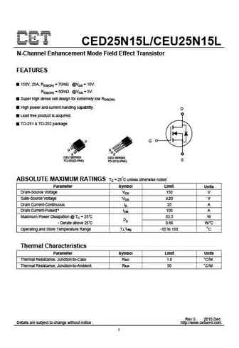
CED25N15L/CEU25N15L N-Channel Enhancement Mode Field Effect Transistor FEATURES 150V, 25A, RDS(ON) = 70m @VGS = 10V. RDS(ON) = 80m @VGS = 5V. Super high dense cell design for extremely low RDS(ON). High power and current handing capability. D Lead free product is acquired. TO-251 & TO-252 package. D G G S CEU SERIES CED SERIES S TO-252(D-PAK) TO-251(I-PAK) ABSOLUTE MAXI
ced25n02 ceu25n02.pdf
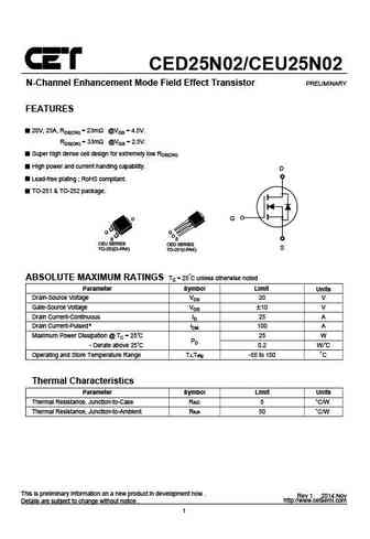
CED25N02/CEU25N02 N-Channel Enhancement Mode Field Effect Transistor PRELIMINARY FEATURES 20V, 25A, RDS(ON) = 23m @VGS = 4.5V. RDS(ON) = 33m @VGS = 2.5V. Super high dense cell design for extremely low RDS(ON). High power and current handing capability. D Lead-free plating ; RoHS compliant. TO-251 & TO-252 package. D G G S CEU SERIES CED SERIES S TO-252(D-PAK) TO-251(I-PA
Otros transistores... CED630N , CED6336 , CED6426 , CED655 , CED730G , CEU16N10 , CEU16N10L , CEU21A2 , P60NF06 , CEU3060 , CEU3100 , CEU3120 , CEU3172 , CEU3252 , CEU4060A , CEU4060AL , CEU40N10 .


Liste
Recientemente añadidas las descripciónes de los transistores:
MOSFET: AOT66613L | AOSP21313C | AOSP21311C | AOB66918L | AO3415C | AOTF20N40L | AOTF11N60L | AOT11N60L | AONS21303C | AOI280A60 | AOB66914L | AO3485C | AOI780A70 | AOB42S60L | AOTF950A70L | AOTF27S60L
Popular searches
2sc2166 | 2sc5198 | 2sc1971 | tip41c transistor datasheet | 2n3907 | 12n60 | mp42b transistor | c1675 transistor