1N90 MOSFET Equivalente. Reemplazo. Hoja de especificaciones. Principales características
Número de Parte: 1N90
Tipo de FET: MOSFET
Polaridad de transistor: N
ESPECIFICACIONES MÁXIMAS
Pdⓘ - Máxima
disipación de potencia: 40 W
|Vds|ⓘ - Voltaje máximo drenador-fuente: 900 V
|Vgs|ⓘ - Voltaje máximo fuente-puerta: 30 V
|Id|ⓘ - Corriente continua
de drenaje: 1 A
Tjⓘ - Temperatura máxima de unión: 150 °C
CARACTERÍSTICAS ELÉCTRICAS
trⓘ - Tiempo
de subida: 15 nS
Cossⓘ - Capacitancia de salida: 22 pF
RDSonⓘ - Resistencia estado encendido drenaje a fuente: 10.3 Ohm
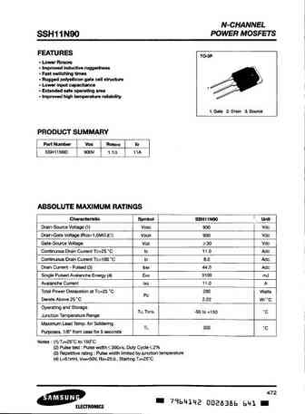
Encapsulados: TO-220
TO-262
TO-251
TO-252
TO-220F
TO-220F1
Búsqueda de reemplazo de 1N90 MOSFET
- Selecciónⓘ de transistores por parámetros
1N90 datasheet
..1. Size:220K utc
1n90.pdf 
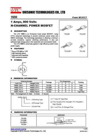
UNISONIC TECHNOLOGIES CO., LTD 1N90 Power MOSFET 1 Amps, 900 Volts N-CHANNEL POWER MOSFET DESCRIPTION The UTC 1N90 is an N-channel mode power MOSFET, using UTC s advanced technology to provide costomers planar stripe and DMOS technology. This technology specializes in allowing a minimum on-state resistance, superior switching performance. It also can withstand high energy
0.1. Size:992K st
stb21n90k5.pdf

STB21N90K5, STF21N90K5, STP21N90K5, STW21N90K5 N-channel 900 V, 0.25 typ., 18.5 A Zener-protected SuperMESH 5 Power MOSFET in a D2PAK, TO-220FP, TO-220 and TO-247 packages Datasheet production data Features TAB Order codes VDSS RDS(on)max ID PW 3 3 1 STB21N90K5 250 W 2 1 D2PAK TO-220FP STF21N90K5 40 W 900 V
0.2. Size:507K st
stb21n90k5 stf21n90k5 stp21n90k5 stw21n90k5.pdf
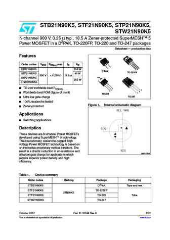
STB21N90K5, STF21N90K5, STP21N90K5, STW21N90K5 N-channel 900 V, 0.25 typ., 18.5 A Zener-protected SuperMESH 5 Power MOSFET in a D2PAK, TO-220FP, TO-220 and TO-247 packages Datasheet production data Features TAB Order codes VDSS RDS(on)max ID PW 3 3 1 STB21N90K5 250 W 2 1 D2PAK TO-220FP STF21N90K5 40 W 900 V
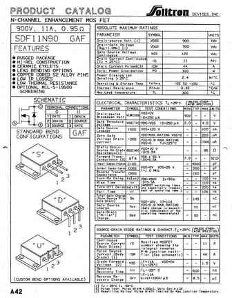
0.3. Size:633K fairchild semi
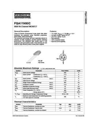
fqaf11n90c.pdf
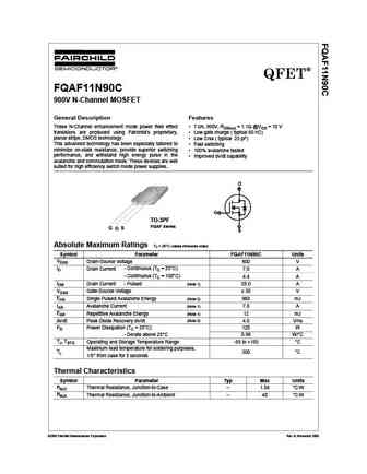
QFET FQAF11N90C 900V N-Channel MOSFET General Description Features These N-Channel enhancement mode power field effect 7.0A, 900V, RDS(on) = 1.1 @VGS = 10 V transistors are produced using Fairchild s proprietary, Low gate charge ( typical 60 nC) planar stripe, DMOS technology. Low Crss ( typical 23 pF) This advanced technology has been especially tailored to Fa
0.4. Size:829K fairchild semi
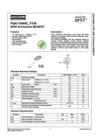
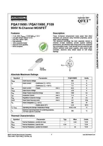
fqa11n90 fqa11n90 f109.pdf

September 2007 QFET FQA11N90 / FQA11N90_F109 900V N-Channel MOSFET Features Description 11.4A, 900V, RDS(on) = 0.96 @VGS = 10 V These N-Channel enhancement mode power field effect Low gate charge ( typical 72 nC) transistors are produced using Fairchild s proprietary, planar stripe, DMOS technology. Low Crss ( typical 30pF) This advanced technology has been especi
0.5. Size:706K fairchild semi
fqa11n90c.pdf

FQA11N90C 900V N-Channel MOSFET General Description Features These N-Channel enhancement mode power field effect 11A, 900V, RDS(on) = 1.1 @VGS = 10 V transistors are produced using Fairchild s proprietary, Low gate charge ( typical 60 nC) planar stripe, DMOS technology. Low Crss ( typical 23 pF) This advanced technology has been especially tailored to Fast switching
0.6. Size:823K fairchild semi
fqa11n90c f109.pdf
September 2007 QFET FQA11N90C_F109 900V N-Channel MOSFET Features Description 11A, 900V, RDS(on) = 1.1 @VGS = 10 V These N-Channel enhancement mode power field effect Low gate charge ( typical 60 nC) transistors are produced using Fairchild s proprietary, planar stripe, DMOS technology. Low Crss ( typical 23pF) This advanced technology has been especially tailored
0.7. Size:827K fairchild semi
fqa11n90.pdf
September 2007 QFET FQA11N90 / FQA11N90_F109 900V N-Channel MOSFET Features Description 11.4A, 900V, RDS(on) = 0.96 @VGS = 10 V These N-Channel enhancement mode power field effect Low gate charge ( typical 72 nC) transistors are produced using Fairchild s proprietary, planar stripe, DMOS technology. Low Crss ( typical 30pF) This advanced technology has been especi
0.8. Size:662K fairchild semi
fqaf11n90.pdf
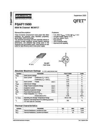
September 2000 TM QFET QFET QFET QFET FQAF11N90 900V N-Channel MOSFET General Description Features These N-Channel enhancement mode power field effect 7.2A, 900V, RDS(on) = 0.96 @ VGS = 10 V transistors are produced using Fairchild s proprietary, Low gate charge ( typical 72 nC) planar stripe, DMOS technology. Low Crss ( typical 30 pF) This advanced technology has
0.9. Size:114K ixys
ixcp01n90e ixcy01n90e.pdf
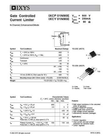
VDSS = 900 V IXCP 01N90E Gate Controlled ID(limit) = 250mA IXCY 01N90E Current Limiter RDS(on)= 80 N-Channel, Enhancement Mode D G S Symbol Test Conditions Maximum Ratings TO-252 (IXCY) VDSS TJ = 25 C to 150 C 900 V TAB VDGR TJ = 25 C to 150 C; RGS = 1 M 900 V G VGS Continuous 20 V S VGSM Transient 30 V PD TC = 25 C40 W TO-220 (IXCP) TJ -55
0.10. Size:708K onsemi
fqa11n90c.pdf
FQA11N90C 900V N-Channel MOSFET General Description Features These N-Channel enhancement mode power field effect 11A, 900V, RDS(on) = 1.1 @VGS = 10 V transistors are produced using Fairchild s proprietary, Low gate charge ( typical 60 nC) planar stripe, DMOS technology. Low Crss ( typical 23 pF) This advanced technology has been especially tailored to Fast switching
0.11. Size:1506K onsemi
fqa11n90-f109.pdf
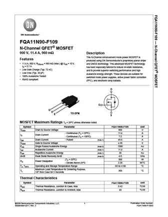
FQA11N90-F109 N-Channel QFET MOSFET 900 V, 11.4 A, 960 m Description This N-Channel enhancement mode power MOSFET is Features produced using ON Semiconductor s proprietary planar stripe 11.4 A, 900 V, RDS(on) = 960 m (Max.) @ VGS = 10 V, and DMOS technology. This advanced MOSFET technology ID = 5.7 A has been especially tailored to reduce on-state resistance, Low
0.12. Size:226K utc
11n90.pdf
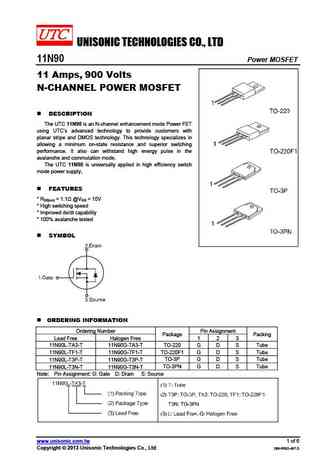
UNISONIC TECHNOLOGIES CO., LTD 11N90 Power MOSFET 11 Amps, 900 Volts N-CHANNEL POWER MOSFET DESCRIPTION The UTC 11N90 is an N-channel enhancement mode Power FET using UTC s advanced technology to provide customers with planar stripe and DMOS technology. This technology specializes in allowing a minimum on-state resistance and superior switching performance. It also can w
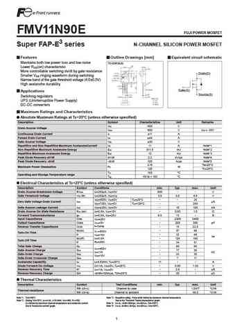
0.13. Size:461K fuji
fmr11n90e.pdf
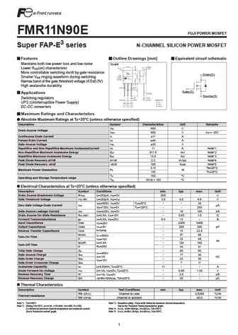
FMR11N90E FUJI POWER MOSFET Super FAP-E3 series N-CHANNEL SILICON POWER MOSFET Features Outline Drawings [mm] Equivalent circuit schematic Maintains both low power loss and low noise TO-3PF Lower R (on) characteristic DS More controllable switching dv/dt by gate resistance Drain(D) Smaller V ringing waveform during switching GS Narrow band of the gate threshold voltage (4.0 0.5V) H
0.14. Size:473K fuji
fmh11n90e.pdf
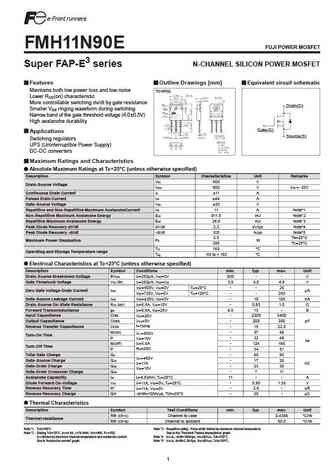
FMH11N90E FUJI POWER MOSFET Super FAP-E3 series N-CHANNEL SILICON POWER MOSFET Features Outline Drawings [mm] Equivalent circuit schematic Maintains both low power loss and low noise TO-3P(Q) Lower R (on) characteristic DS More controllable switching dv/dt by gate resistance Drain(D) Smaller V ringing waveform during switching GS Narrow band of the gate threshold voltage (4.0 0.5V)
0.15. Size:455K fuji
fmv11n90e.pdf
FMV11N90E FUJI POWER MOSFET Super FAP-E3 series N-CHANNEL SILICON POWER MOSFET Features Outline Drawings [mm] Equivalent circuit schematic Maintains both low power loss and low noise TO-220F(SLS) Lower R (on) characteristic DS More controllable switching dv/dt by gate resistance Drain(D) Smaller V ringing waveform during switching GS Narrow band of the gate threshold voltage (4.0 0.
0.17. Size:146K jiangsu
cjb71n90.pdf
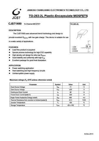
JIANGSU CHANGJIANG ELECTRONICS TECHNOLOGY CO., LTD TO-263-2L Plastic-Encapsulate MOSFETS CJB71N90 N-Channel MOSFET TO-263-2L DESCRIPTION The CJB71N90 uses advanced trench technology and design to provide excellent RDS(ON) with low gate charge .This device is suitable for use in a wide variety of applications. 1. GATE FEATURES 2. DRAIN Lead free product is acquired 3
0.18. Size:132K jiangsu
cjp71n90.pdf
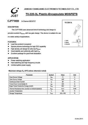
JIANGSU CHANGJIANG ELECTRONICS TECHNOLOGY CO., LTD T0-220-3L Plastic-Encapsulate MOSFETS CJP71N90 N-Channel MOSFET TO-220-3L DESCRIPTION The CJP71N90 uses advanced trench technology and design to provide excellent RDS(ON) with low gate charge .This device is suitable for use in a wide variety of applications. 1. GATE FEATURES 2. DRAIN 3. SOURCE Lead free product is
0.19. Size:1513K jilin sino
jcs11n90wt jcs11n90abt.pdf
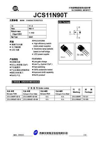
N R N-CHANNEL MOSFET JCS11N90T MAIN CHARACTERISTICS Package ID 11 A VDSS 900 V Rdson-max 1.10 Vgs=10V Qg-typ 66nC APPLICATIONS High efficiency switch mode power supplies Electronic lamp ballasts LED based on half bridge LE
0.23. Size:187K semihow
hfh11n90.pdf
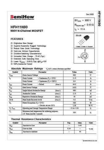
Dec 2005 BVDSS = 900 V RDS(on) typ HFH11N90 ID = 11 A 900V N-Channel MOSFET TO-3P FEATURES 1 Originative New Design 2 3 Superior Avalanche Rugged Technology 1.Gate 2. Drain 3. Source Robust Gate Oxide Technology Very Low Intrinsic Capacitances Excellent Switching Characteristics Unrivalled Gate Charge 75 nC (Typ.) Extended Safe Operating Area Lower RDS(ON
0.24. Size:512K trinnotech
tman11n90z.pdf
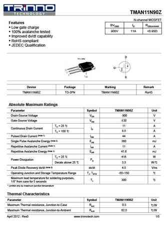
TMAN11N90Z N-channel MOSFET Features BVDSS ID RDS(on)MAX Low gate charge 900V 11A
0.25. Size:508K trinnotech
tman11n90az.pdf
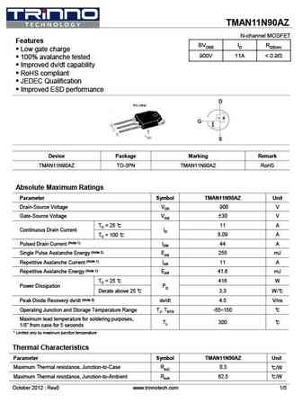
TMAN11N90AZ N-channel MOSFET Features BVDSS ID RDS(on) Low gate charge 900V 11A
0.26. Size:544K convert
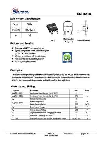
cs11n90v cs11n90vf.pdf
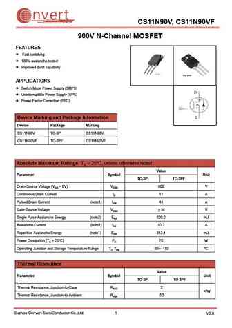
nvert Suzhou Convert Semiconductor Co ., Ltd. CS11N90V, CS11N90VF 900V N-Channel MOSFET FEATURES Fast switching 100% avalanche tested Improved dv/dt capability APPLICATIONS Switch Mode Power Supply (SMPS) Uninterruptible Power Supply (UPS) Power Factor Correction (PFC) Device Marking and Package Information Device Package Marking CS11N90V TO-3P CS11N90V CS
0.27. Size:1821K first semi
fir11n90ang.pdf
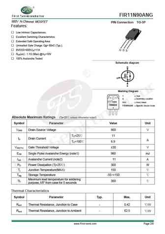
FIR11N90ANG 900V N-Channel MOSFET PIN Connection TO-3P Features Low Intrinsic Capacitances. Excellent Switching Characteristics. Extended Safe Operating Area. Unrivalled Gate Charge Qg= 60nC (Typ.). BVDSS=900V,ID=11A RDS(on) 1.1 (Max) @VG=10V 100% Avalanche Tested g Schematic dia ram D G S Marking Diagram Y = Year A = Assembly Location
0.28. Size:286K inchange semiconductor
fqa11n90.pdf
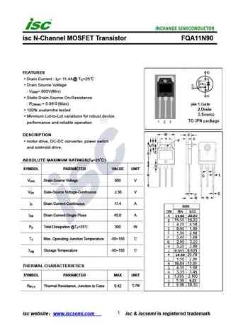
isc N-Channel MOSFET Transistor FQA11N90 FEATURES Drain Current I = 11.4A@ T =25 D C Drain Source Voltage V = 900V(Min) DSS Static Drain-Source On-Resistance R = 0.96 (Max) DS(on) 100% avalanche tested Minimum Lot-to-Lot variations for robust device performance and reliable operation DESCRIPTION motor drive, DC-DC converter, power switch and solenoid drive.
Otros transistores... SUM202MN
, 8N90
, 9N90
, 10N90
, 11N90
, 12N90
, 9N95
, 9N100
, IRF3710
, 2N90
, 3N90
, 4N90
, 5N90
, 6N90
, 7N90
, 1N80
, 2N80
.