7N80 MOSFET Equivalente. Reemplazo. Hoja de especificaciones. Principales características
Número de Parte: 7N80
Tipo de FET: MOSFET
Polaridad de transistor: N
ESPECIFICACIONES MÁXIMAS
Pdⓘ - Máxima disipación de potencia: 142 W
|Vds|ⓘ - Voltaje máximo drenador-fuente: 800 V
|Vgs|ⓘ - Voltaje máximo fuente-puerta: 30 V
|Id|ⓘ - Corriente continua de drenaje: 7 A
Tjⓘ - Temperatura máxima de unión: 150 °C
CARACTERÍSTICAS ELÉCTRICAS
trⓘ - Tiempo de subida: 100 nS
Cossⓘ - Capacitancia de salida: 120 pF
RDSonⓘ - Resistencia estado encendido drenaje a fuente: 1.4 Ohm
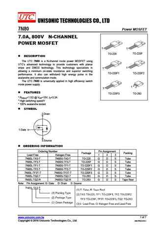
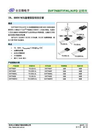
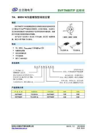
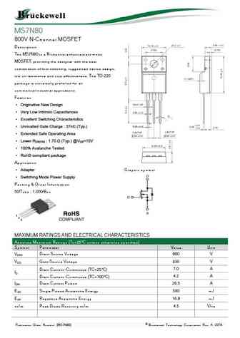
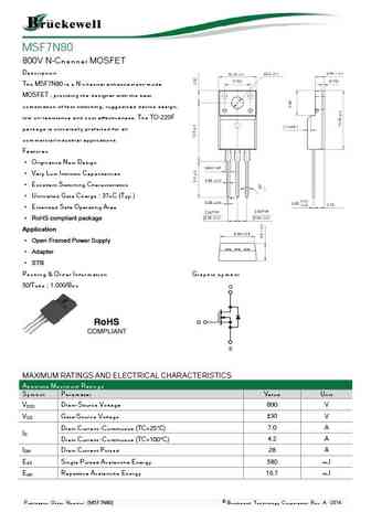
Encapsulados: TO-263 TO-220 TO-220F TO-220F1 TO-220F2
Búsqueda de reemplazo de 7N80 MOSFET
- Selecciónⓘ de transistores por parámetros
7N80 datasheet
7n80.pdf
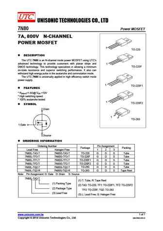
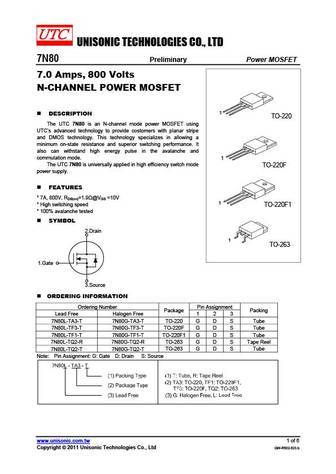
UNISONIC TECHNOLOGIES CO., LTD 7N80 Power MOSFET 7A, 800V N-CHANNEL POWER MOSFET 1 TO-220 DESCRIPTION The UTC 7N80 is an N-channel mode power MOSFET using UTC s advanced technology to provide customers with planar stripe and 1 TO-220F DMOS technology. This technology specializes in allowing a minimum on-state resistance and superior switching performance. It also can
7n80.pdf
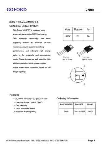
GOFORD 7N80 800V N-Channel MOSFET GENERAL DESCRIPTION VDSS RDS(ON) ID This Power MOSFET is produced using advanced planar stripe DMOS technology. 800V 2 7A This advanced technology has been especially tailored to minimize on-state resistance, provide superior switching performance, and withstand high energy pulse in the avalanche and commutation mode. These devices are well sui
7n80l-t 7n80g-t.pdf
UNISONIC TECHNOLOGIES CO., LTD 7N80 Preliminary Power MOSFET 7.0 Amps, 800 Volts N-CHANNEL POWER MOSFET 1 DESCRIPTION TO-220 The UTC 7N80 is an N-channel mode power MOSFET using UTC s advanced technology to provide costomers with planar stripe and DMOS technology. This technology specializes in allowing a minimum on-state resistance and superior switching performance. It a
mtw7n80erev3.pdf
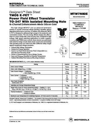
MOTOROLA Order this document SEMICONDUCTOR TECHNICAL DATA by MTW7N80E/D Designer's Data Sheet MTW7N80E TMOS E-FET. Motorola Preferred Device Power Field Effect Transistor TO-247 With Isolated Mounting Hole TMOS POWER FET N Channel Enhancement Mode Silicon Gate 7.0 AMPERES 800 VOLTS This high voltage MOSFET uses an advanced termination RDS(on) = 1.0 OHM scheme to provide
mtw7n80e.pdf
MOTOROLA Order this document SEMICONDUCTOR TECHNICAL DATA by MTW7N80E/D Designer's Data Sheet MTW7N80E TMOS E-FET. Motorola Preferred Device Power Field Effect Transistor TO-247 With Isolated Mounting Hole TMOS POWER FET N Channel Enhancement Mode Silicon Gate 7.0 AMPERES 800 VOLTS This high voltage MOSFET uses an advanced termination RDS(on) = 1.0 OHM scheme to provide
stf7n80k5 stfi7n80k5.pdf
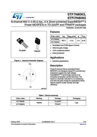
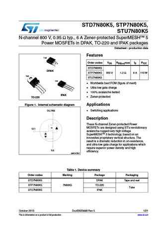
STF7N80K5, STFI7N80K5 N-channel 800 V, 0.95 typ., 6 A Zener-protected SuperMESH 5 Power MOSFETs in TO-220FP and I2PAKFP packages Datasheet - production data Features Order codes VDS RDS(on)max ID PTOT STF7N80K5 800 V 1.2 6 A 25 W STFI7N80K5 Worldwide best FOM (figure of merit) 3 2 Ultra low gate charge 1 1 2 3 TO-220FP 100% avalanche tested I 2PAKFP
stb17n80k5.pdf
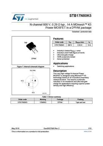
STB17N80K5 N-channel 800 V, 0.29 typ., 14 A MDmesh K5 Power MOSFET in a D PAK package Datasheet - production data Features Order code V R max. I DS DS(on) D TAB STB17N80K5 800 V 0.34 14 A 2 Industry s lowest RDS(on) x area 3 Industry s best FoM (figure of merit) 1 Ultra-low gate charge 100% avalanche tested D PAK Zener-protected
stl7n80k5.pdf
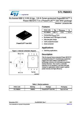
STL7N80K5 N-channel 800 V, 0.95 typ., 3.6 A Zener-protected SuperMESH 5 Power MOSFET in a PowerFLAT 5x6 VHV package Datasheet - production data Features Order code VDS RDS(on)max. ID STL7N80K5 800 V 1.2 3.6 A Outstanding RDS(on)*area 1 Worldwide best FOM (figure of merit) 2 3 Ultra low gate charge 4 100% avalanche tested PowerFLAT 5x6 VHV Zener
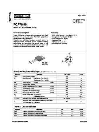
fqaf7n80.pdf
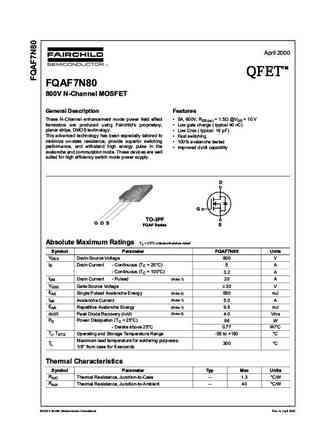
April 2000 TM QFET QFET QFET QFET 800V N-ChanneI MOSFET GeneraI Description Features These N-Channel enhancement mode power field effect 5A, 800V, RDS(on) = 1.5 @VGS = 10 V transistors are produced using Fairchild s proprietary, Low gate charge ( typical 40 nC) planar stripe, DMOS technology. Low Crss ( typical 19 pF) This advanced technology has been esp
fqa7n80c.pdf
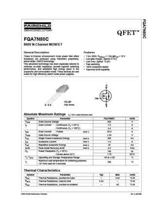
TM QFET FQA7N80C 800V N-Channel MOSFET General Description Features These N-Channel enhancement mode power field effect 7.0A, 800V, RDS(on) = 1.9 @VGS = 10 V transistors are produced using Fairchild s proprietary, Low gate charge ( typical 27 nC) planar stripe, DMOS technology. Low Crss ( typical 10 pF) This advanced technology has been especially tailored to Fast
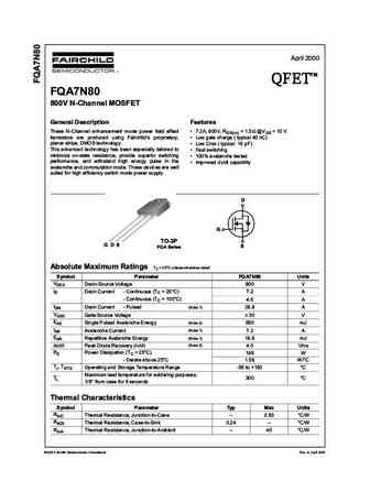
fqa7n80.pdf
April 2000 TM QFET QFET QFET QFET 800V N-ChanneI MOSFET GeneraI Description Features These N-Channel enhancement mode power field effect 7.2A, 800V, RDS(on) = 1.5 @VGS = 10 V transistors are produced using Fairchild s proprietary, Low gate charge ( typical 40 nC) planar stripe, DMOS technology. Low Crss ( typical 19 pF) This advanced technology has been es
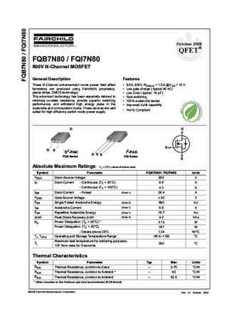
fqb7n80tm am002 fqi7n80tu fqi7n80 fqb7n80.pdf
October 2008 QFET FQB7N80 / FQI7N80 800V N-ChanneI MOSFET GeneraI Description Features These N-Channel enhancement mode power field effect 6.6A, 800V, RDS(on) = 1.5 @VGS = 10 V transistors are produced using Fairchild s proprietary, Low gate charge ( typical 40 nC) planar stripe, DMOS technology. Low Crss ( typical 19 pF) This advanced technology has been especially
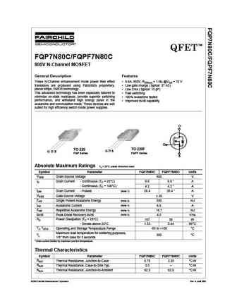
fqp7n80c fqpf7n80c.pdf
TM QFET FQP7N80C/FQPF7N80C 800V N-Channel MOSFET General Description Features These N-Channel enhancement mode power field effect 6.6A, 800V, RDS(on) = 1.9 @VGS = 10 V transistors are produced using Fairchild s proprietary, Low gate charge ( typical 27 nC) planar stripe, DMOS technology. Low Crss ( typical 10 pF) This advanced technology has been especially tailored to
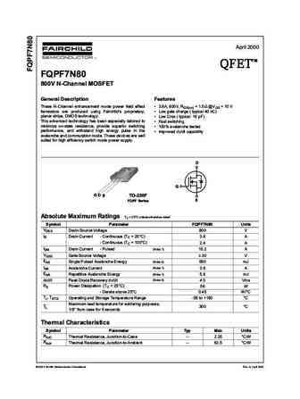
fqpf7n80.pdf
April 2000 TM QFET QFET QFET QFET 800V N-ChanneI MOSFET GeneraI Description Features These N-Channel enhancement mode power field effect 3.8A, 800V, RDS(on) = 1.5 @VGS = 10 V transistors are produced using Fairchild s proprietary, Low gate charge ( typical 40 nC) planar stripe, DMOS technology. Low Crss ( typical 19 pF) This advanced technology has been e
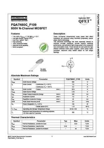
fqa7n80c f109.pdf
September 2007 QFET FQA7N80C_F109 800V N-Channel MOSFET Features Description 7.0A, 800V, RDS(on) = 1.9 @VGS = 10 V These N-Channel enhancement mode power field effect Low gate charge ( typical 27nC) transistors are produced using Fairchild s proprietary, planar stripe, DMOS technology. Low Crss ( typical 10pF) This advanced technology has been especially tailored
fqp7n80.pdf
April 2000 TM QFET QFET QFET QFET 800V N-ChanneI MOSFET GeneraI Description Features These N-Channel enhancement mode power field effect 6.6A, 800V, RDS(on) = 1.5 @VGS = 10 V transistors are produced using Fairchild s proprietary, Low gate charge ( typical 40 nC) planar stripe, DMOS technology. Low Crss ( typical 19 pF) This advanced technology has been es
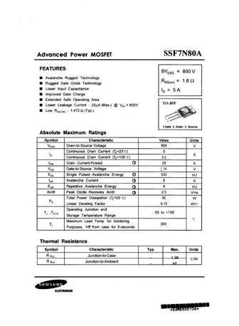
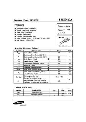
sss7n80a.pdf
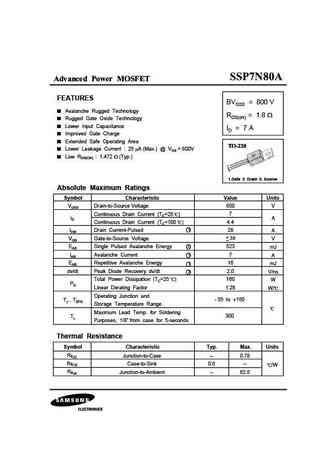
Advanced Power MOSFET FEATURES BVDSS = 800 V Avalanche Rugged Technology RDS(on) = 1.8 Rugged Gate Oxide Technology Lower Input Capacitance ID = 4 A Improved Gate Charge Extended Safe Operating Area Lower Leakage Current 25 A (Max.) @ VDS = 800V Low RDS(ON) 1.472 (Typ.) 1 2 3 1.Gate 2. Drain 3. Source Absolute Maximum Ratings Symbol Characteristic Value
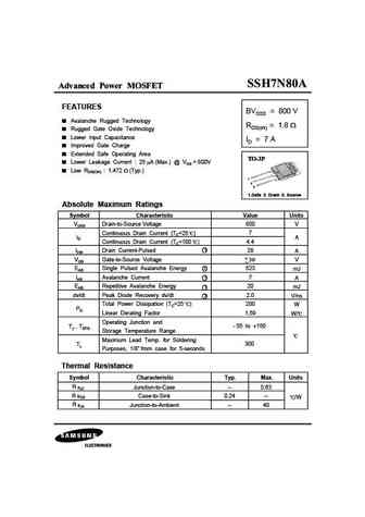
ssh7n80a.pdf
Advanced Power MOSFET FEATURES BVDSS = 800 V Avalanche Rugged Technology RDS(on) = 1.8 Rugged Gate Oxide Technology Lower Input Capacitance ID = 7 A Improved Gate Charge Extended Safe Operating Area Lower Leakage Current 25 A (Max.) @ VDS = 800V Low RDS(ON) 1.472 (Typ.) 1 2 3 1.Gate 2. Drain 3. Source Absolute Maximum Ratings Symbol Characteristic Value
ssp7n80a.pdf
Advanced Power MOSFET FEATURES BVDSS = 800 V Avalanche Rugged Technology RDS(on) = 1.8 Rugged Gate Oxide Technology Lower Input Capacitance ID = 7 A Improved Gate Charge Extended Safe Operating Area Lower Leakage Current 25 A (Max.) @ VDS = 800V Low RDS(ON) 1.472 (Typ.) 1 2 3 1.Gate 2. Drain 3. Source Absolute Maximum Ratings Symbol Characteristic Value
sihg17n80e.pdf
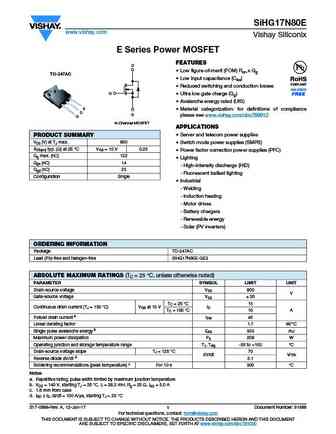
SiHG17N80E www.vishay.com Vishay Siliconix E Series Power MOSFET FEATURES D Low figure-of-merit (FOM) Ron x Qg TO-247AC Low input capacitance (Ciss) Reduced switching and conduction losses G Ultra low gate charge (Qg) Avalanche energy rated (UIS) S Material categorization for definitions of compliance D S please see www.vishay.com/doc?99912 G N-Chann
sihp17n80e.pdf
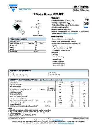
SiHP17N80E www.vishay.com Vishay Siliconix E Series Power MOSFET FEATURES D Low figure-of-merit (FOM) Ron x Qg TO-220AB Low input capacitance (Ciss) Reduced switching and conduction losses G Ultra low gate charge (Qg) Avalanche energy rated (UIS) Material categorization for definitions of compliance S D S please see www.vishay.com/doc?99912 G N-Chann
spw17n80c3.pdf
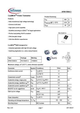
SPW17N80C3 CoolMOSTM Power Transistor Product Summary Features V 800 V DS New revolutionary high voltage technology R @ Tj = 25 C 0.29 DS(on)max Extreme dv/dt rated Q 88 nC g,typ High peak current capability Qualified according to JEDEC1) for target applications PG-TO247-3 Pb-free lead plating; RoHS compliant Ultra low gate charge Ultra low eff
spp17n80c3 spa17n80c3.rev.2.7.pdf
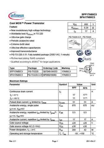
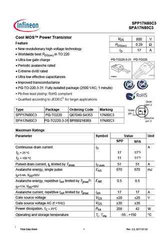
SPP17N80C3 SPA17N80C3 Cool MOS Power Transistor VDS 800 V Feature RDS(on) 0.29 New revolutionary high voltage technology ID 17 A Worldwide best RDS(on) in TO 220 PG-TO220-3-31 PG-TO220 Ultra low gate charge Periodic avalanche rated 3 Extreme dv/dt rated 2 1 P-TO220-3-31 Ultra low effective capacitances Improved transconductance PG-TO-22
spb17n80c3.pdf
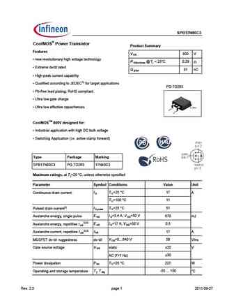
SPB17N80C3 CoolMOS Power Transistor Product Summary Features V 800 V DS new revolutionary high voltage technology R @ Tj = 25 C 0.29 DS(on)max Extreme dv/dt rated Q 91 nC g,typ High peak current capability Qualified according to JEDEC1) for target applications PG-TO263 Pb-free lead plating; RoHS compliant Ultra low gate charge Ultra low effec
spp17n80c3.pdf
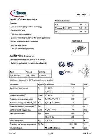
SPP17N80C3 CoolMOS Power Transistor Product Summary Features V 800 V DS New revolutionary high voltage technology R @ Tj = 25 C 0.29 DS(on)max Extreme dv/dt rated Q 88 nC g,typ High peak current capability Qualified according to JEDEC1) for target applications PG-TO220-3 Pb-free lead plating; RoHS compliant Ultra low gate charge Ultra low eff
spp17n80c3 spa17n80c3.pdf
SPP17N80C3 SPA17N80C3 Cool MOS Power Transistor VDS 800 V Feature RDS(on) 0.29 New revolutionary high voltage technology ID 17 A Worldwide best RDS(on) in TO 220 PG-TO220-3-31 PG-TO220 Ultra low gate charge Periodic avalanche rated 3 Extreme dv/dt rated 2 1 P-TO220-3-31 Ultra low effective capacitances Improved transconductance PG-TO-22
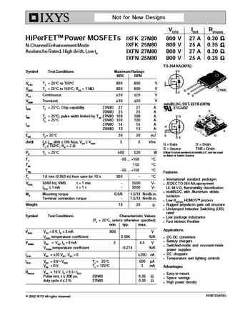
ixfk25n80 ixfk27n80 ixfn25n80 ixfn27n80.pdf
Not for New Designs VDSS ID25 RDS(on) IXFK 27N80 800 V 27 A 0.30 HiPerFETTM Power MOSFETs IXFK 25N80 800 V 25 A 0.35 N-Channel Enhancement Mode Avalanche Rated, High dv/dt, Low trr IXFN 27N80 800 V 27 A 0.30 IXFN 25N80 800 V 25 A 0.35 TO-264 AA (IXFK) Symbol Test Conditions Maximum Ratings
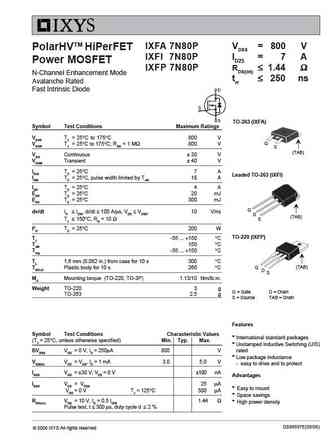
ixfi7n80p.pdf
IXFA 7N80P VDSS = 800 V PolarHVTM HiPerFET IXFI 7N80P ID25 = 7 A Power MOSFET IXFP 7N80P RDS(on) 1.44 N-Channel Enhancement Mode trr 250 ns Avalanche Rated Fast Intrinsic Diode TO-263 (IXFA) Symbol Test Conditions Maximum Ratings VDSS TJ = 25 C to 175 C 800 V G VDGR TJ = 25 C to 175 C; RGS = 1 M 800 V S (TAB) V
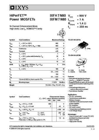
ixfh7n80 ixfm7n80.pdf
HiPerFETTM IXFH 7 N80 VDSS = 800 V Power MOSFETs IXFM 7 N80 ID (cont) = 7 A RDS(on) = 1.4 W N-Channel Enhancement Mode trr = 250 ns High dv/dt, Low trr, HDMOSTM Family Symbol Test Conditions Maximum Ratings TO-247 AD (IXFH) VDSS TJ = 25 C to 150 C 800 V VDGR TJ = 25 C to 150 C; RGS = 1 MW 800 V (TAB) VGS Continuous 20 V VGSM Transient 30 V ID25 TC = 25 C7 A TO-204 AA (IXFM
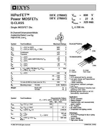
ixfk27n80q ixfx27n80q.pdf
VDSS = 800 V HiPerFETTM IXFK 27N80Q IXFX 27N80Q ID25 = 27 A Power MOSFETs RDS(on) = 320 m Q-CLASS trr 250 ns Single MOSFET Die N-Channel Enhancement Mode Avalanche Rated, Low Qg, High dV/dt, Low trr Symbol Test Conditions Maximum Ratings PLUS 247TM (IXFX) VDSS TJ = 25 C to 150 C 800 V VDGR TJ = 25 C to 150 C; RGS = 1 M 800 V
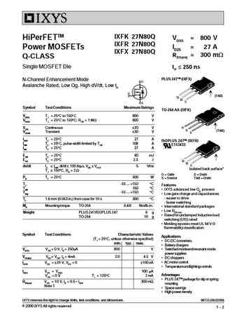
ixfr27n80q.pdf
IXFK 27N80Q HiPerFETTM VDSS = 800 V IXFR 27N80Q ID25 = 27 A Power MOSFETs IXFX 27N80Q RDS(on) = 300 mW Q-CLASS Single MOSFET Die trr 250 ns PLUS 247TM (IXFX) N-Channel Enhancement Mode Avalanche Rated, Low Qg, High dV/dt, Low trr (TAB) G D Symbol Test Conditions Maximum Ratings TO-264 AA (IXFK) VDSS TJ = 25 C to 150 C 800 V VDGR TJ = 25 C to 150 C; RGS = 1 MW 800 V G
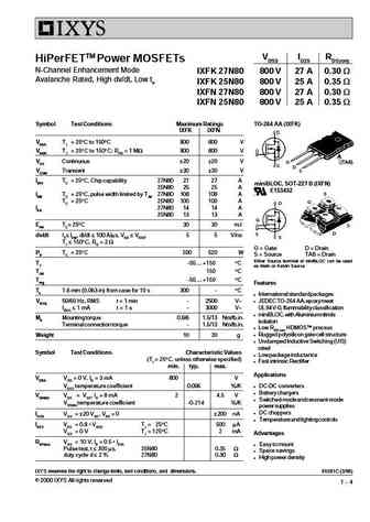
ixfk27n80 ixfn27n80 ixfk25n80 ixfn25n80.pdf
VDSS ID25 RDS(on) HiPerFETTM Power MOSFETs N-Channel Enhancement Mode IXFK 27N80 800 V 27 A 0.30 W Avalanche Rated, High dv/dt, Low trr IXFK 25N80 800 V 25 A 0.35 W IXFN 27N80 800 V 27 A 0.30 W IXFN 25N80 800 V 25 A 0.35 W Symbol Test Conditions Maximum Ratings TO-264 AA (IXFK) IXFK IXFN VDSS TJ = 25 C to 150 C 800 800 V VDGR TJ = 25 C to 150 C; RGS = 1 MW 800 800 V VGS Continuo
fqi7n80.pdf
Is Now Part of To learn more about ON Semiconductor, please visit our website at www.onsemi.com Please note As part of the Fairchild Semiconductor integration, some of the Fairchild orderable part numbers will need to change in order to meet ON Semiconductor s system requirements. Since the ON Semiconductor product management systems do not have the ability to manage part nomenclatur
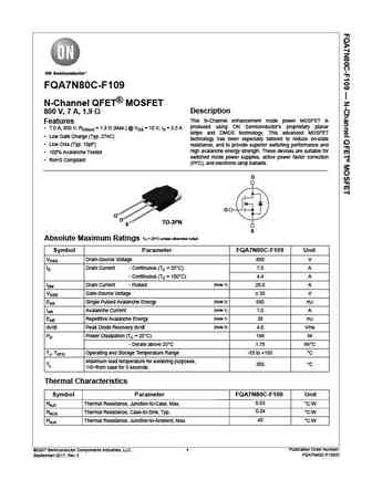
fqa7n80c-f109.pdf
FQA7N80C-F109 N-Channel QFET MOSFET Description 800 V, 7 A, 1.9 This N-Channel enhancement mode power MOSFET is Features produced using ON Semiconductor s proprietary planar 7.0 A, 800 V, RDS(on) = 1.9 (Max.) @ VGS = 10 V, ID = 3.5 A stripe and DMOS technology. This advanced MOSFET Low Gate Charge (Typ. 27nC) technology has been especially tailored to reduce o
fqp7n80c fqpf7n80c.pdf
TM QFET FQP7N80C/FQPF7N80C 800V N-Channel MOSFET General Description Features These N-Channel enhancement mode power field effect 6.6A, 800V, RDS(on) = 1.9 @VGS = 10 V transistors are produced using Fairchild s proprietary, Low gate charge ( typical 27 nC) planar stripe, DMOS technology. Low Crss ( typical 10 pF) This advanced technology has been especially tailored to
7n80l-ta3-t 7n80g-ta3-t 7n80l-tf3-t 7n80g-tf3-t 7n80l-tf1-t 7n80g-tf1-t 7n80l-tf2-t 7n80g-tf2-t 7n80l-tf3t-t 7n80g-tf3t-t 7n80l-tq2-t 7n80g-tq2-t 7n80l-tq2-r 7n80g-tq2-r.pdf
UNISONIC TECHNOLOGIES CO., LTD 7N80 Power MOSFET 7.0A, 800V N-CHANNEL POWER MOSFET 1 1 TO-220 TO-220F DESCRIPTION The UTC 7N80 is a N-channel mode power MOSFET using UTC s advanced technology to provide customers with planar stripe and DMOS technology. This technology specializes in 1 1 allowing a minimum on-state resistance and superior switching TO-220F1 TO-220F2 pe
apt17n80bc3g apt17n80sc3g.pdf
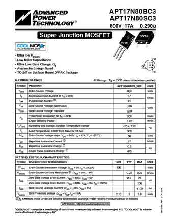
APT17N80BC3 APT17N80SC3 800V 17A 0.290 D3PAK Super Junction MOSFET TO-247 COOLMOS Power Semiconductors Ultra low RDS(ON) D Low Miller Capacitance Ultra Low Gate Charge, Qg G Avalanche Energy Rated S TO-247 or Surface Mount D3PAK Package MAXIMUM RATINGS All Ratings TC = 25 C unless otherwise specified. Symbol Parameter APT17N80BC3_SC
apt17n80sc3.pdf
APT17N80BC3 APT17N80SC3 800V 17A 0.290 D3PAK Super Junction MOSFET TO-247 COOLMOS Power Semiconductors Ultra low RDS(ON) D Low Miller Capacitance Ultra Low Gate Charge, Qg G Avalanche Energy Rated S TO-247 or Surface Mount D3PAK Package MAXIMUM RATINGS All Ratings TC = 25 C unless otherwise specified. Symbol Parameter APT17N80BC3_SC
apt17n80bc3.pdf
APT17N80BC3 APT17N80SC3 800V 17A 0.290 D3PAK Super Junction MOSFET TO-247 COOLMOS Power Semiconductors Ultra low RDS(ON) D Low Miller Capacitance Ultra Low Gate Charge, Qg G Avalanche Energy Rated S TO-247 or Surface Mount D3PAK Package MAXIMUM RATINGS All Ratings TC = 25 C unless otherwise specified. Symbol Parameter APT17N80BC3_SC
kf7n80p-f.pdf
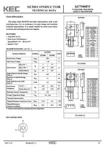
KF7N80P/F SEMICONDUCTOR N CHANNEL MOS FIELD TECHNICAL DATA EFFECT TRANSISTOR General Description KF7N80P A This planar stripe MOSFET has better characteristics, such as fast O C switching time, low on resistance, low gate charge and excellent F avalanche characteristics. It is mainly suitable for active power factor E DIM MILLIMETERS G _ correction and switching mode power supp
sif7n80c.pdf
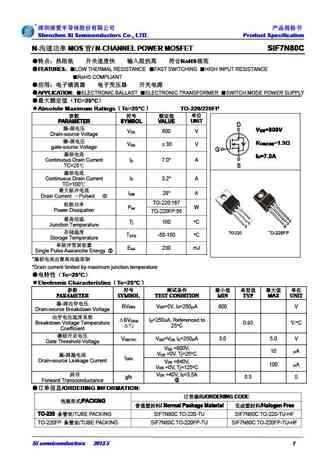
Shenzhen SI Semiconductors Co., LTD. Product Specification Shenzhen SI Semiconductors Co., LTD. Product Specification Shenzhen SI Semiconductors Co., LTD. Product Specification Shenzhen SI Semiconductors Co., LTD. Product Specification N- MOS / N-CHANNEL POWER MOSFET SIF7N80C N- MOS / N-CHANNEL POWER MOSFET SIF7N80C N- MOS / N-CHANN
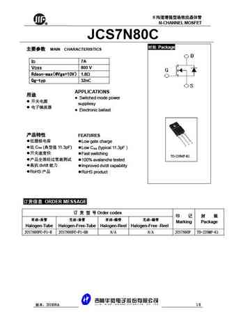
jcs7n80fh jcs7n80ch jcs7n80bh jcs7n80sh.pdf
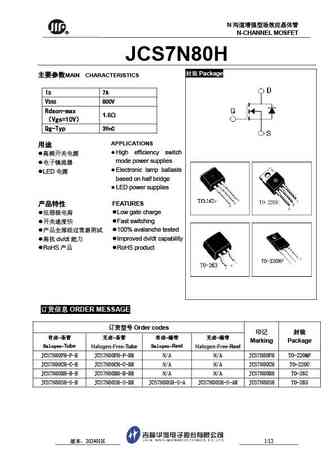
N R N-CHANNEL MOSFET JCS7N80H Package MAIN CHARACTERISTICS ID 7A VDSS 800V Rdson-max 1.6 Vgs=10V Qg-Typ 39nC APPLICATIONS High efficiency switch mode power supplies Electronic lamp ballasts LED based on half bridge LED po
7n80f.pdf
GOFORD 7N80 800V N-Channel MOSFET GENERAL DESCRIPTION VDSS RDS(ON) ID This Power MOSFET is produced using advanced planar stripe DMOS technology. 800V 2 7A This advanced technology has been especially tailored to minimize on-state resistance, provide superior switching performance, and withstand high energy pulse in the avalanche and commutation mode. These devices are well sui
sdf07n80 sdp07n80.pdf
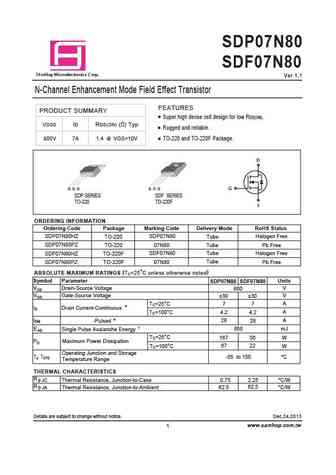
SDP07N80 SDF07N80 a S mHop Microelectronics C orp. Ver 1.1 N-Channel Enhancement Mode Field Effect Transistor FEATURES PRODUCT SUMMARY Super high dense cell design for low RDS(ON). RDS(ON) ( ) Typ VDSS ID Rugged and reliable. 800V 7A 1.4 @ VGS=10V TO-220 and TO-220F Package. D G D S G D S G SDP SERIES SDF SERIES TO-220 TO-220F S ORDERING INFORMATION Ordering Code Package Mar
brb7n80.pdf
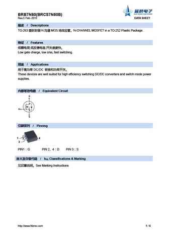
BRB7N80(BRCS7N80B) Rev.C Feb.-2015 DATA SHEET / Descriptions TO-263 N MOS N-CHANNEL MOSFET in a TO-252 Plastic Package. / Features , , Low gate charge, low crss, fast switching. / Applications DC/DC These devices are well suited for high
brf7n80.pdf
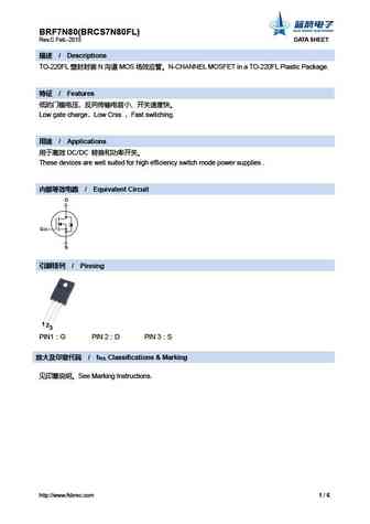
BRF7N80(BRCS7N80FL) Rev.C Feb.-2015 DATA SHEET / Descriptions TO-220FL N MOS N-CHANNEL MOSFET in a TO-220FL Plastic Package. / Features Low gate charge Low Crss Fast switching. / Applications DC/DC These devices are
br7n80.pdf
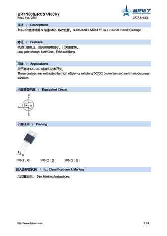
BR7N80(BRCS7N80R) Rev.C Feb.-2015 DATA SHEET / Descriptions TO-220 N MOS N-CHANNEL MOSFET in a TO-220 Plastic Package. / Features Low gate charge, Low Crss , Fast switching. / Applications DC/DC These devices are well su
brfl7n80.pdf
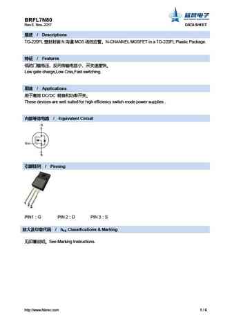
BRFL7N80 Rev.E. Nov.-2017 DATA SHEET / Descriptions TO-220FL N MOS N-CHANNEL MOSFET in a TO-220FL Plastic Package. / Features Low gate charge,Low Crss,Fast switching. / Applications DC/DC These devices are well suited fo
bra7n80.pdf
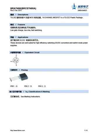
BRA7N80(BRCS7N80A) Rev.C Feb.-2015 DATA SHEET / Descriptions TO-262 N MOS N-CHANNEL MOSFET in a TO-252 Plastic Package.. / Features , , Low gate charge, low crss, fast switching. / Applications DC/DC These devices are well suited for high
hfp7n80.pdf
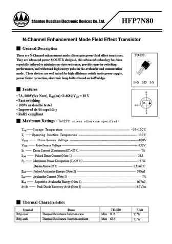
Shantou Huashan Electronic Devices Co., Ltd. HFP7N80 N-Channel Enhancement Mode Field Effect Transistor General Description These are N-Channel enhancement mode silicon gate power field effect transistors. TO-220 They are advanced power MOSFETs designed, this advanced technology has been especially tailored to minimize on-state resistance, provide superior switching performan
cs7n80 a8.pdf
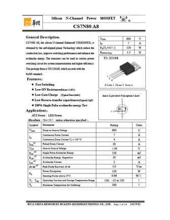
Silicon N-Channel Power MOSFET R CS7N80 A8 General Description VDSS 800 V CS7N80 A8, the silicon N-channel Enhanced VDMOSFETs, is ID 7 A PD(TC=25 ) 120 W obtained by the self-aligned planar Technology which reduce the RDS(ON)Typ 1.5 conduction loss, improve switching performance and enhance the avalanche energy. The transistor can be used in various power sw
cs7n80f a9.pdf
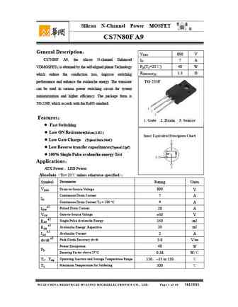
Silicon N-Channel Power MOSFET R CS7N80F A9 General Description VDSS 800 V CS7N80F A9, the silicon N-channel Enhanced ID 7 A PD(TC=25 ) 48 W VDMOSFETs, is obtained by the self-aligned planar Technology RDS(ON)Typ 1.5 which reduce the conduction loss, improve switching performance and enhance the avalanche energy. The transistor can be used in various power
f7n80.pdf
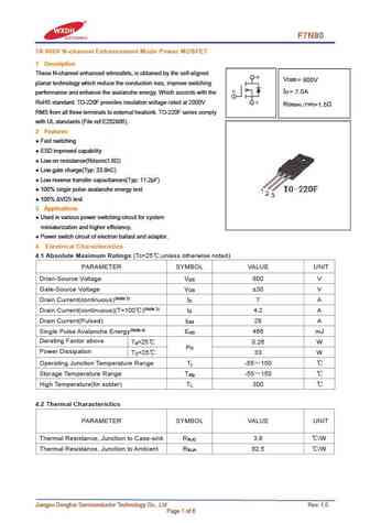
F7N80 7A 800V N-channel Enhancement Mode Power MOSFET 1 Description These N-channel enhanced vdmosfets, is obtained by the self-aligned V DSS = 800V planar technology which reduce the conduction loss, improve switching I = 7.0A D performance and enhance the avalanche energy. Which accords with the RoHS standard. TO-220F provides insulation voltage rated at 2000V R DS(on) TYP) =1.
svf7n80t svf7n80f.pdf
SVF7N80T/F 7A 800V N 2 SVF7N80T/F N MOS F-CellTM VDMOS 1 3 AC-DC
ms7n80.pdf
MS7N80 800V N-Channel MOSFET Description The MS7N80 is a N-channel enhancement-mode MOSFET, providing the designer with the best combination of fast switching, ruggedized device design, low on-resistance and cost effectiveness. The TO-220 package is universally preferred for all commercial-industrial applications Features Originative New Design Very Low Intrinsic C
msf7n80.pdf
MSF7N80 800V N-Channel MOSFET Description The MSF7N80 is a N-channel enhancement-mode MOSFET , providing the designer with the best combination of fast switching, ruggedized device design, low on-resistance and cost effectiveness. The TO-220F package is universally preferred for all commercial-industrial applications Features Originative New Design Very Low Intrins
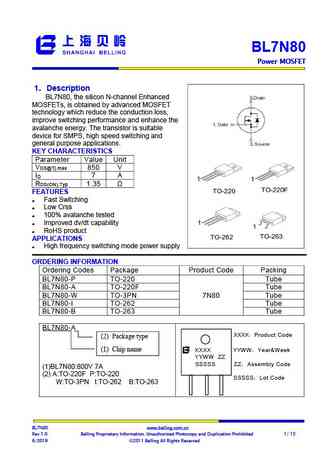
bl7n80-p bl7n80-a bl7n80-w bl7n80-i bl7n80-b.pdf
BL7N80 Power MOSFET Power MOSFET Power MOSFET Power MOSFET 1 Description BL7N80, the silicon N-channel Enhanced MOSFETs, is obtained by advanced MOSFET technology which reduce the conduction loss, improve switching performance and enhance the avalanche energy. The transistor is suitable device for SMPS, high speed switching and general purpose application
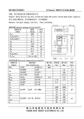
cs7n80f.pdf
BRF7N80(CS7N80F) N-Channel MOSFET/N MOS DC/DC Purpose These devices are well suited for high efficiency switch mode power supplies. Features Low gate charge Low Crss Fast switching. /Absolute maximum ratings(Ta=25 )
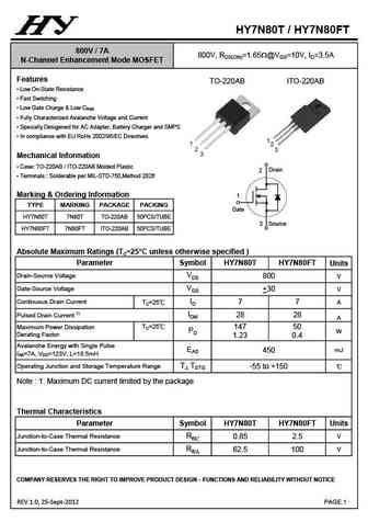
hy7n80t.pdf
SINGLE FIG.SINGLE PHASE HALF WAVE 60Hz DERATING CURVE FIG. 2 MAXIMUM NON- T1 FORWARD CURRENT AMBIENT TEMPERATURE ( ) 1 2 5 10 1 25 50 75 10 20 150 175 0.00 0.2 0.4 0.6 4 100 125 100 HY7N80T / HY7N80FT 800V / 7A 800V, RDS(ON)=1.65W@VGS=10V, ID=3.5A N-Channel Enhancement Mode MOSFET Features TO-220AB ITO-220AB Low On-State Resistance Fast Switching L
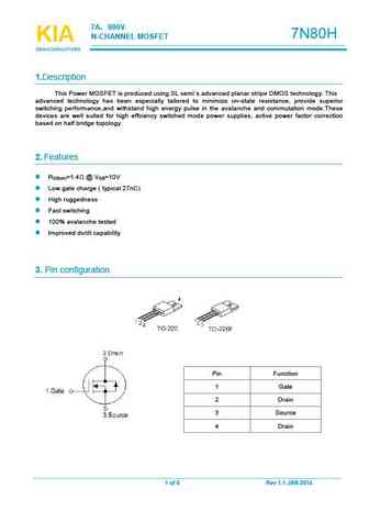
kia7n80h.pdf
7A 800V 7N80H N-CHANNELMOSFET KIA KIA KIA SEMICONDUCTORS SEMICONDUCTORS SEMICONDUCTORS 1.Description This Power MOSFETis produced using SLsemi s advanced planar stripeDMOStechnology. This advanced technology has been especially tailored to minimize on-state resistance, provide superior switching performance,and withstand high energy pulse in the avalanche and commutation mode.Thes
slp7n80c slf7n80c.pdf
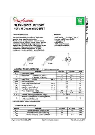
SLP7N80C/SLF7N80C SLP7N80C/SLF7N80C 800V N-Channel MOSFET General Description Features This Power MOSFET is produced using Maple semi s - 7.0A, 800V, RDS(on) = 1.9 @VGS = 10 V advanced planar stripe DMOS technology. - Low gate charge ( typical 40nC) This advanced technology has been especially tailored - High ruggedness to minimize on-state resistance, provide superior switching Fast
ptf27n80.pdf
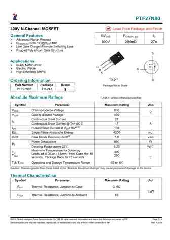
PTF27N80 800V N-Channel MOSFET General Features BVDSS RDS(ON),typ. ID Advanced Planar Process 800V 280m 27A RDS(ON),typ.=280 m @VGS=10V Low Gate Charge Minimize Switching Loss Rugged Poly silicon Gate Structure Applications BLDC Motor Driver Electric Welder High Efficiency SMPS Ordering Information Part Number Package Brand PTF27N80 TO-247 Absolute Max
swf17n80k swp17n80k.pdf
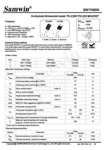
SW17N80K N-channel Enhanced mode TO-220F/TO-220 MOSFET TO-220F TO-220 BVDSS 800V Features ID 17A High ruggedness RDS(ON) 0.31 Low RDS(ON) (Typ 0.31 )@VGS=10V Low Gate Charge (Typ 57nC) 2 Improved dv/dt Capability 1 1 100% Avalanche Tested 2 2 1 3 3 Application LED , Charger, SMPS 1. Gate 2. Drain 3. Source 3 General Descr
sw7n80d swf7n80d swu7n80d swj7n80d.pdf
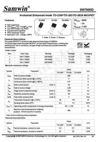
SW7N80D N-channel Enhanced mode TO-220F/TO-262/TO-262N MOSFET TO-220F TO-262 TO-262N BVDSS 800V Features ID 7A High ruggedness RDS(ON) 1.5 Low RDS(ON) (Typ 1.5 )@VGS=10V Low Gate Charge (Typ 39nC) 2 Improved dv/dt Capability 1 1 1 100% Avalanche Tested 2 2 2 1 3 3 3 Application LED , Charger, SMPS 1. Gate 2. Drain 3. Source
swf7n80d swu7n80d swj7n80d.pdf
SW7N80D N-channel Enhanced mode TO-220F/TO-262/TO-262N MOSFET TO-220F TO-262 TO-262N BVDSS 800V Features ID 7A High ruggedness RDS(ON) 1.5 Low RDS(ON) (Typ 1.5 )@VGS=10V Low Gate Charge (Typ 39nC) 2 Improved dv/dt Capability 1 1 1 100% Avalanche Tested 2 2 2 1 3 3 3 Application LED , Charger, SMPS 1. Gate 2. Drain 3. Source
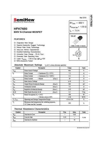
hfh7n80.pdf
Mar 2010 BVDSS = 800 V RDS(on) typ = 1.55 HFH7N80 ID = 7.0 A 800V N-Channel MOSFET TO-3P FEATURES 1 Originative New Design 2 3 Superior Avalanche Rugged Technology 1.Gate 2. Drain 3. Source Robust Gate Oxide Technology Very Low Intrinsic Capacitances Excellent Switching Characteristics Unrivalled Gate Charge 35 nC (Typ.) Unrivalled Gate Charge 35 nC (Typ ) Exte
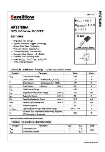
hfs7n80a.pdf
June 2021 BVDSS = 800 V RDS(on) Typ = 1.55 HFS7N80A ID = 7.0 A 800V N-Channel MOSFET TO-220F FEATURES Originative New Design Superior Avalanche Rugged Technology 1 2 3 Robust Gate Oxide Technology 1.Gate 2. Drain 3. Source Very Low Intrinsic Capacitances Excellent Switching Characteristics Unrivalled Gate Charge 40 nC (Typ.) Extended Safe Oper
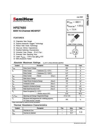
hfs7n80.pdf
July 2005 BVDSS = 800 V RDS(on) typ = 1.55 HFS7N80 ID = 7.0 A 800V N-Channel MOSFET TO-220F FEATURES 1 Originative New Design 2 3 Superior Avalanche Rugged Technology 1.Gate 2. Drain 3. Source Robust Gate Oxide Technology Very Low Intrinsic Capacitances Excellent Switching Characteristics Unrivalled Gate Charge 35 nC (Typ.) Unrivalled Gate Charge 35 nC (Typ ) E
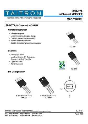
msk7n80f msk7n80t.pdf
800V/7A N-Channel MOSFET MSK7N80T/F 800V/7A N-Channel MOSFET General Description Fast switching time Low on resistance, low gate charge Excellent avalanche characteristics Suitable for electronic ballast Suitable for switching mode power supplies TO-220 Features VDSS=800V, ID=7A; Low Drain-Source ON Resistance RDS(ON) =1.55 @ VGS=10V
tsp7n80m tsf7n80m.pdf
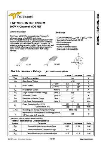
TSP7N80M/TSF7N80M 800V N-Channel MOSFET General Description Features This Power MOSFET is produced using Truesemi s 7.0A,800V,Max.RDS(on)=1.6 @ VGS =10V advanced planar stripe DMOS technology. This advanced technology has been especially tailored to Low gate charge(typical 40nC) minimize on-state resistance, provide superior switching High ruggedness performance, and
wmj27n80d1.pdf
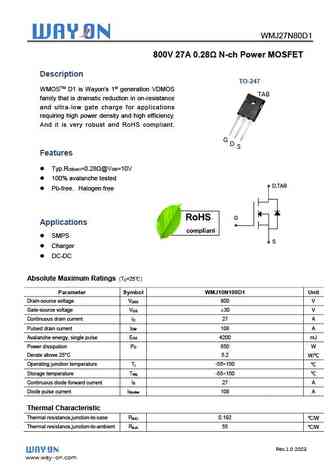
WMJ27N80D1 800V 27A 0.28 N-ch Power MOSFET Description TO-247 WMOSTM D1 is Wayon s 1st generation VDMOS TAB family that is dramatic reduction in on-resistance and ultra-low gate charge for applications requiring high power density and high efficiency. And it is very robust and RoHS compliant. G D S Features Typ.R =0.28 @V =10V DS(on) GS 100% avalanch
wml07n80m3 wmn07n80m3 wmm07n80m3 wmo07n80m3 wmp07n80m3 wmk07n80m3.pdf
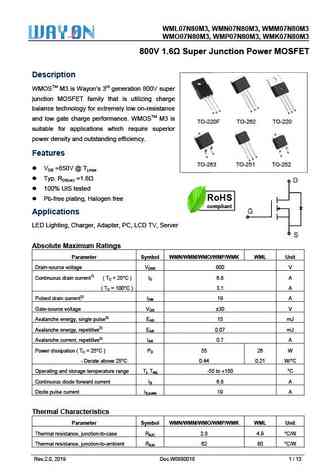
WML07N80M3, W 80M3, WM M3 WMN07N8 MM07N80M WMO0 80M3, WM M3 07N80M3, WMP07N8 MK07N80M 800 Junction ET 0V 1.6 Super J n Power MOSFE Descrip ption WMOSTM M3 is Wayo neration 800 M on s 3rd gen 0V super junction MOSFET fa that is utilizing charge M amily S balance te or extremely esistance D echnology fo y low on-re S S G D D G G G T and low ga charge perf
wml7n80d1.pdf
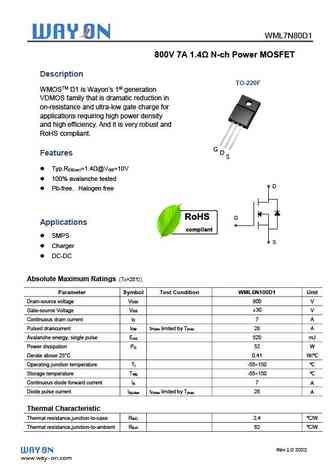
WML7N80D1 800V 7A 1.4 N-ch Power MOSFET Description TO-220F WMOSTM D1 is Wayon s 1st generation VDMOS family that is dramatic reduction in on-resistance and ultra-low gate charge for applications requiring high power density and high efficiency. And it is very robust and RoHS compliant. G D Features S Typ.R =1.4 @V =10V DS(on) GS 100% avalanche tested
wml07n80m3 wmm07n80m3 wmo07n80m3 wmp07n80m3 wmk07n80m3 wmn07n80m3.pdf
WML07N80M3, W 80M3, WM M3 WMN07N8 MM07N80M WMO0 80M3, WM M3 07N80M3, WMP07N8 MK07N80M 800 Junction ET 0V 1.6 Super J n Power MOSFE Descrip ption WMOSTM M3 is Wayo neration 800 M on s 3rd gen 0V super junction MOSFET fa that is utilizing charge M amily S balance te or extremely esistance D echnology fo y low on-re S S G D D G G G T and low ga charge perf
cs7n80a8.pdf
Silicon N-Channel Power MOSFET R CS7N80 A8 General Description VDSS 800 V CS7N80 A8, the silicon N-channel Enhanced VDMOSFETs, is ID 7 A PD(TC=25 ) 120 W obtained by the self-aligned planar Technology which reduce the RDS(ON)Typ 1.5 conduction loss, improve switching performance and enhance the avalanche energy. The transistor can be used in various power sw
cs7n80fa9.pdf
Silicon N-Channel Power MOSFET R CS7N80F A9 General Description VDSS 800 V CS7N80F A9, the silicon N-channel Enhanced ID 7 A PD(TC=25 ) 48 W VDMOSFETs, is obtained by the self-aligned planar Technology RDS(ON)Typ 1.5 which reduce the conduction loss, improve switching performance and enhance the avalanche energy. The transistor can be used in various power
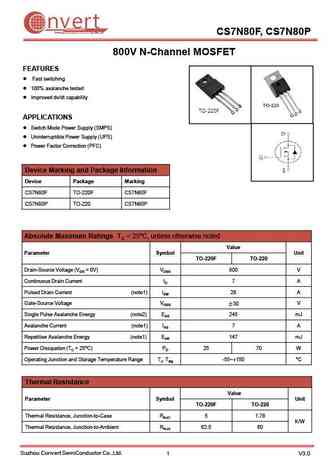
cs7n80f cs7n80p.pdf
nvert Suzhou Convert Semiconductor Co ., Ltd. CS7N80F, CS7N80P 800V N-Channel MOSFET FEATURES Fast switching 100% avalanche tested Improved dv/dt capability APPLICATIONS Switch Mode Power Supply (SMPS) Uninterruptible Power Supply (UPS) Power Factor Correction (PFC) Device Marking and Package Information Device Package Marking CS7N80F TO-220F CS7N80F CS7N8
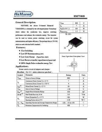
hm7n80d.pdf
HM7N80D General Description VDSS 800 V , the silicon N-channel Enhanced ID 7 A PD(TC=25 ) 185 W VDMOSFETs, is obtained by the self-aligned planar Technology RDS(ON)Typ 1.5 which reduce the conduction loss, improve switching performance and enhance the avalanche energy. The transistor can be used in various power switching circuit for system miniaturization
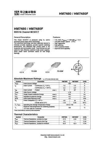
hm7n80 hm7n80f.pdf
HM7N80 / HM7N80F HM7N80 / HM7N80F 800V N-Channel MOSFET General Description Features This Power MOSFET is produced using SL semi s 7.0A, 800V, RDS(on) = 1.90 @VGS = 10 V advanced planar stripe DMOS technology. Low gate charge ( typical 27nC) This advanced technology has been especially tailored to High ruggedness minimize on-state resistance, provide superior switchin
sfp070n80c2 sfb067n80c2.pdf
SFP070N80C2, SFB067N80C2 N-MOSFET 80V, 6.0m , 118A Product Summary General Description VDS 80V Trench Power technology Low RDS(ON) RDS(on) 6.0m Low Gate Charge ID 118A Optimized for fast-switching applications 100% DVDS Tested Applications 100% Avalanche Tested 100% Avalanche Tested 100% Avalanche Tested 100% Avalanche Tested 100% Avalanche Tested S
sfp090n80c2 sfb087n80c2.pdf
SFP090N80C2,SFB087N80C2 N-MOSFET 80V, 7.4m , 80A Features Product Summary Extremely low on-resistance RDS(on) VDS 80V Excellent QgxRDS(on) product(FOM) RDS(on) typ. 7.4m Qualified according to JEDEC criteria ID 80A 100% DVDS Tested Applications 100% Avalanche Tested Motor control and drive Battery management UPS (Uninterrupible Power Supplies) SFP09
spa17n80c3.pdf
isc N-Channel MOSFET Transistor SPA17N80C3 FEATURES Static drain-source on-resistance RDS(on) 0.29 Enhancement mode Fast Switching Speed 100% avalanche tested Minimum Lot-to-Lot variations for robust device performance and reliable operation APPLICATIONS Ideal for high-frequency switching and synchronous rectification ABSOLUTE MAXIMUM RATINGS(T =25 ) a SY
spw17n80c3.pdf
isc N-Channel MOSFET Transistor SPW17N80C3 ISPW17N80C3 FEATURES Static drain-source on-resistance RDS(on) 290m Enhancement mode 100% avalanche tested Minimum Lot-to-Lot variations for robust device performance and reliable operation DESCRITION High peak current capability ABSOLUTE MAXIMUM RATINGS(T =25 ) a SYMBOL PARAMETER VALUE UNIT V Drain-Source Voltag
fqpf7n80c.pdf
isc N-Channel MOSFET Transistor FQPF7N80C FEATURES Drain-source on-resistance RDS(on) 1.9 @10V Fast Switching Speed 100% avalanche tested Minimum Lot-to-Lot variations for robust device performance and reliable operation APPLICATIONS High efficiency switch mode power supplies. ABSOLUTE MAXIMUM RATINGS(T =25 ) a SYMBOL PARAMETER VALUE UNIT V Drain-Source Vol
spb17n80c3.pdf
Isc N-Channel MOSFET Transistor SPB17N80C3 FEATURES With To-263(D2PAK) package Low input capacitance and gate charge Low gate input resistance 100% avalanche tested Minimum Lot-to-Lot variations for robust device performance and reliable operation APPLICATIONS Switching applications ABSOLUTE MAXIMUM RATINGS(T =25 ) a SYMBOL PARAMETER VALUE UNIT V Drain-Source Vo
spp17n80c3.pdf
isc N-Channel MOSFET Transistor SPP17N80C3 ISPP17N80C3 FEATURES Static drain-source on-resistance RDS(on) 0.29 Enhancement mode Fast Switching Speed 100% avalanche tested Minimum Lot-to-Lot variations for robust device performance and reliable operation DESCRIPTION High peak current capability Ultra low gate charge Ultra low effective capacitances ABS
std7n80k5.pdf
isc N-Channel MOSFET Transistor STD7N80K5 FEATURES Static drain-source on-resistance RDS(on) 1.2 100% avalanche tested Minimum Lot-to-Lot variations for robust device performance and reliable operation DESCRITION Switching applications ABSOLUTE MAXIMUM RATINGS(T =25 ) a SYMBOL PARAMETER VALUE UNIT V Drain-Source Voltage 800 V DSS V Gate-Source Voltage 30 V
Otros transistores... 6N90, 7N90, 1N80, 2N80, 3N80, 4N80, 5N80, 6N80, STP75NF75, 8N80, 9N80, 10N80, 12N80, 1N70Z, 2N70, 2N70Z, 2N70ZL
🌐 : EN ES РУ
Liste
Recientemente añadidas las descripciónes de los transistores:
MOSFET: AUP060N055 | AUP056N10 | AUP056N08BGL | AUP052N085 | AUP045N12 | AUP039N10 | AUP034N10 | AUP034N06 | AUP033N08BG | AUP026N085 | AUN084N10 | AUN065N10 | AUN063N10 | AUN062N08BG | AUN060N08AG | AUN053N10
Popular searches
2sc945 transistor | c2073 transistor | ac176 transistor | mpsa20 | irfp264 | ksc2690 | bc546 datasheet | mpsa06 transistor
