1N60 MOSFET Equivalente. Reemplazo. Hoja de especificaciones. Principales características
Número de Parte: 1N60
Tipo de FET: MOSFET
Polaridad de transistor: N
ESPECIFICACIONES MÁXIMAS
Pdⓘ - Máxima disipación de potencia: 40 W
|Vds|ⓘ - Voltaje máximo drenador-fuente: 600 V
|Vgs|ⓘ - Voltaje máximo fuente-puerta: 30 V
|Id|ⓘ - Corriente continua de drenaje: 1.2 A
Tjⓘ - Temperatura máxima de unión: 150 °C
CARACTERÍSTICAS ELÉCTRICAS
trⓘ - Tiempo de subida: 25 nS
Cossⓘ - Capacitancia de salida: 20 pF
RDSonⓘ - Resistencia estado encendido drenaje a fuente: 9.3 Ohm
Encapsulados: TO-220 TO-92 SOT-223 TO-126 TO-251 TO-252
Búsqueda de reemplazo de 1N60 MOSFET
- Selecciónⓘ de transistores por parámetros
1N60 datasheet
1n60.pdf
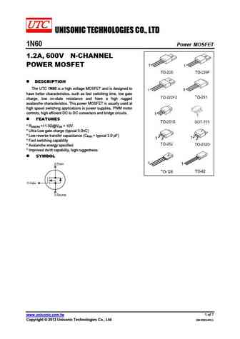
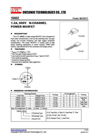
UNISONIC TECHNOLOGIES CO., LTD 1N60 Power MOSFET 1.2A, 600V N-CHANNEL POWER MOSFET DESCRIPTION The UTC 1N60 is a high voltage MOSFET and is designed to have better characteristics, such as fast switching time, low gate charge, low on-state resistance and have a high rugged avalanche characteristics. This power MOSFET is usually used at high speed switching applications in
1n60.pdf
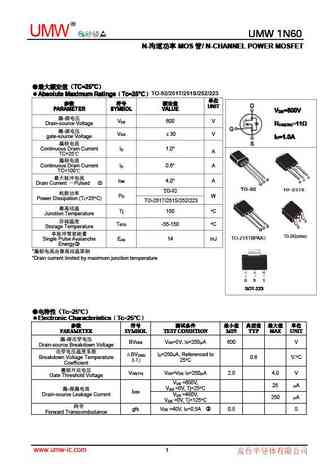
R UMW UMW 1N60 UMW 1N60 UMW 1N60 N- MOS / N-CHANNEL POWER MOSFET N- MOS / N-CHANNEL POWER MOSFET N- MOS / N-CHANNEL POWER MOSFET N- MOS / N-CHANNEL POWER MOSFET TC=25 C TC=25 C TC=25 C TC=25 C Absolute Maximum Ratings Tc=25 C Absolute Maximum Ratings Tc=25 C Absolute Maximum Ratings Tc=25 C TO-92/251T/251S/252/2
spd01n60c3 spu01n60c3.pdf
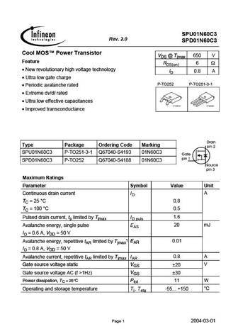
SPU01N60C3 Rev. 2.0 SPD01N60C3 Cool MOS Power Transistor VDS @ Tjmax 650 V Feature RDS(on) 6 New revolutionary high voltage technology ID 0.8 A Ultra low gate charge P-TO252 P-TO251-3-1 Periodic avalanche rated Extreme dv/dt rated Ultra low effective capacitances Improved transconductance Type Package Ordering Code Marking SPU01N60C3 P-TO251-3-1 Q6
mtd1n60e.pdf
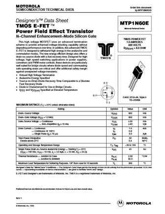
MOTOROLA Order this document SEMICONDUCTOR TECHNICAL DATA by MTD1N60E/D Designer's Data Sheet MTD1N60E TMOS E-FET. Motorola Preferred Device Power Field Effect Transistor DPAK for Surface Mount TMOS POWER FET N Channel Enhancement Mode Silicon Gate 1.0 AMPERE 600 VOLTS This high voltage MOSFET uses an advanced termination RDS(on) = 8.0 OHM scheme to provide enhanced vol
mtp1n60erev1x.pdf

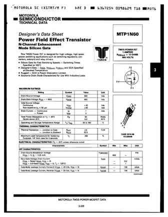
MOTOROLA Order this document SEMICONDUCTOR TECHNICAL DATA by MTP1N60E/D Designer's Data Sheet MTP1N60E TMOS E-FET. Motorola Preferred Device Power Field Effect Transistor N Channel Enhancement Mode Silicon Gate TMOS POWER FET This high voltage MOSFET uses an advanced termination 1.0 AMPERES scheme to provide enhanced voltage blocking capability without 600 VOLTS degra
mgw21n60edrev0.pdf
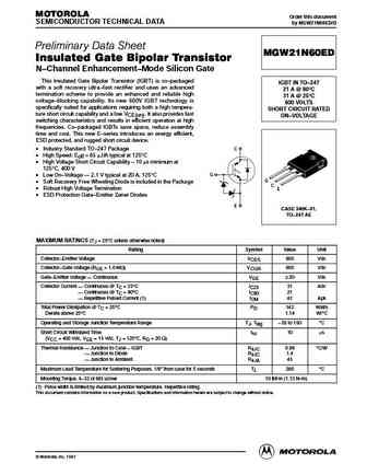
MOTOROLA Order this document SEMICONDUCTOR TECHNICAL DATA by MGW21N60ED/D Preliminary Data Sheet MGW21N60ED Insulated Gate Bipolar Transistor N Channel Enhancement Mode Silicon Gate This Insulated Gate Bipolar Transistor (IGBT) is co packaged IGBT IN TO 247 with a soft recovery ultra fast rectifier and uses an advanced 21 A @ 90 C termination scheme to provide an enhanced
mtp1n60e.pdf
MOTOROLA Order this document SEMICONDUCTOR TECHNICAL DATA by MTP1N60E/D Designer's Data Sheet MTP1N60E TMOS E-FET. Motorola Preferred Device Power Field Effect Transistor N Channel Enhancement Mode Silicon Gate TMOS POWER FET This high voltage MOSFET uses an advanced termination 1.0 AMPERES scheme to provide enhanced voltage blocking capability without 600 VOLTS degra
mgp11n60de.pdf
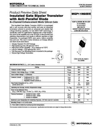
MOTOROLA Order this document SEMICONDUCTOR TECHNICAL DATA by MGP11N60DE/D Product Preview Data Sheet MGP11N60DE Insulated Gate Bipolar Transistor with Anti-Parallel Diode IGBT & DIODE IN TO 220 N Channel Enhancement Mode Silicon Gate 11 A @ 90 C This Insulated Gate Bipolar Transistor (IGBT) is co packaged 15 A @ 25 C with a soft recovery ultra fast rectifier and uses an ad
mgw21n60ed.pdf
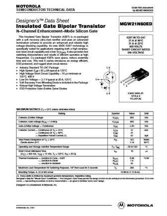
MOTOROLA Order this document SEMICONDUCTOR TECHNICAL DATA by MGW21N60ED/D Designer's Data Sheet MGW21N60ED Insulated Gate Bipolar Transistor N Channel Enhancement Mode Silicon Gate This Insulated Gate Bipolar Transistor (IGBT) is co packaged IGBT IN TO 247 with a soft recovery ultra fast rectifier and uses an advanced 21 A @ 90 C termination scheme to provide an enhanc
mgp21n60erev0.pdf

MOTOROLA Order this document SEMICONDUCTOR TECHNICAL DATA by MGP21N60E/D Designer's Data Sheet MGP21N60E Insulated Gate Bipolar Transistor N Channel Enhancement Mode Silicon Gate This Insulated Gate Bipolar Transistor (IGBT) uses an advanced IGBT IN TO 220 termination scheme to provide an enhanced and reliable high 21 A @ 90 C voltage blocking capability. Its new 600 V I
mgp11n60erev0.pdf
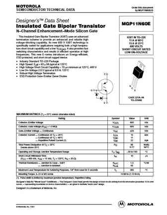
MOTOROLA Order this document SEMICONDUCTOR TECHNICAL DATA by MGP11N60E/D Designer's Data Sheet MGP11N60E Insulated Gate Bipolar Transistor N Channel Enhancement Mode Silicon Gate This Insulated Gate Bipolar Transistor (IGBT) uses an advanced IGBT IN TO 220 termination scheme to provide an enhanced and reliable high 11 A @ 90 C voltage blocking capability. Its new 600 V I
mgp21n60e.pdf

MOTOROLA Order this document SEMICONDUCTOR TECHNICAL DATA by MGP21N60E/D Designer's Data Sheet MGP21N60E Insulated Gate Bipolar Transistor N Channel Enhancement Mode Silicon Gate This Insulated Gate Bipolar Transistor (IGBT) uses an advanced IGBT IN TO 220 termination scheme to provide an enhanced and reliable high 21 A @ 90 C voltage blocking capability. Its new 600 V I
mgp11n60ed.pdf
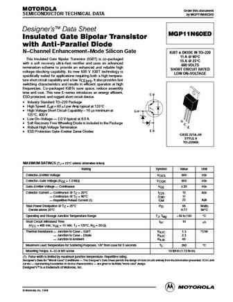
MOTOROLA Order this document SEMICONDUCTOR TECHNICAL DATA by MGP11N60ED/D Designer's Data Sheet MGP11N60ED Insulated Gate Bipolar Transistor with Anti-Parallel Diode N Channel Enhancement Mode Silicon Gate IGBT & DIODE IN TO 220 11 A @ 90 C This Insulated Gate Bipolar Transistor (IGBT) is co packaged 15 A @ 25 C with a soft recovery ultra fast rectifier and uses an a
irfr1n60a.pdf
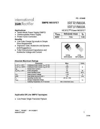
PD - 91846B SMPS MOSFET IRFR1N60A IRFU1N60A Applications HEXFET Power MOSFET l Switch Mode Power Supply (SMPS) VDSS Rds(on) max ID l Uninterruptable Power Supply l Power Factor Correction 600V 7.0 1.4A Benefits l Low Gate Charge Qg results in Simple Drive Requirement l Improved Gate, Avalanche and dynamic dv/dt Ruggedness l Fully Characterized Capacitance and Avalanche Vol
irfr1n60apbf irfu1n60apbf.pdf
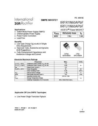
PD - 95518A SMPS MOSFET IRFR1N60APbF IRFU1N60APbF Applications HEXFET Power MOSFET l Switch Mode Power Supply (SMPS) VDSS Rds(on) max ID l Uninterruptable Power Supply l Power Factor Correction 600V 7.0 1.4A l Lead-Free Benefits l Low Gate Charge Qg results in Simple Drive Requirement l Improved Gate, Avalanche and dynamic dv/dt Ruggedness l Fully Characterized Capacitance
irfr1n60apbf irfu1n60apbf.pdf
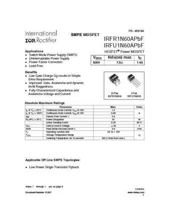
PD - 95518A SMPS MOSFET IRFR1N60APbF IRFU1N60APbF Applications HEXFET Power MOSFET l Switch Mode Power Supply (SMPS) VDSS Rds(on) max ID l Uninterruptable Power Supply l Power Factor Correction 600V 7.0 1.4A l Lead-Free Benefits l Low Gate Charge Qg results in Simple Drive Requirement l Improved Gate, Avalanche and dynamic dv/dt Ruggedness l Fully Characterized Capacitance
irfp21n60lpbf.pdf
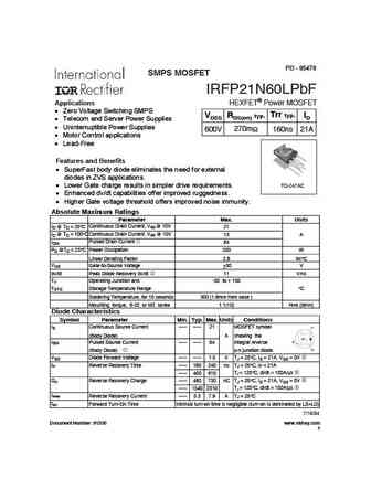
PD - 95478 SMPS MOSFET IRFP21N60LPbF Applications HEXFET Power MOSFET Zero Voltage Switching SMPS Trr typ. VDSS RDS(on) typ. ID Telecom and Server Power Supplies Uninterruptible Power Supplies 600V 270m 160ns 21A Motor Control applications Lead-Free Features and Benefits SuperFast body diode eliminates the need for external diodes in ZVS applications.
irfp21n60l.pdf
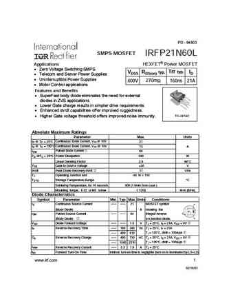
PD - 94503 SMPS MOSFET IRFP21N60L Applications HEXFET Power MOSFET Zero Voltage Switching SMPS Trr typ. VDSS RDS(on) typ. ID Telecom and Server Power Supplies Uninterruptible Power Supplies 600V 270m 160ns 21A Motor Control applications Features and Benefits SuperFast body diode eliminates the need for external diodes in ZVS applications. Lower Gate ch
pht1n60r 4.pdf
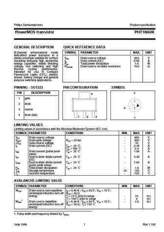
Philips Semiconductors Product specification PowerMOS transistor PHT1N60R GENERAL DESCRIPTION QUICK REFERENCE DATA N-channel enhancement mode SYMBOL PARAMETER MAX. UNIT field-effect power transistor in a plastic envelope suitable for surface VDS Drain-source voltage 600 V mounting featuring high avalanche ID Drain current (DC) 0.46 A energy capability, stable blocking Ptot Total power
php1n60e 1.pdf
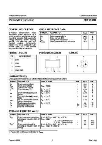
Philips Semiconductors Objective Specification PowerMOS transistor PHP1N60E GENERAL DESCRIPTION QUICK REFERENCE DATA N-channel enhancement mode SYMBOL PARAMETER MAX. UNIT field-effect power transistor in a plastic envelope featuring high VDS Drain-source voltage 600 V avalanche energy capability, stable ID Drain current (DC) 1.9 A blocking voltage, fast switching and Ptot Total power d
pht1n60p.pdf
Philips Semiconductors Objective specification PowerMOS transistor PHT1N60R GENERAL DESCRIPTION QUICK REFERENCE DATA N-channel enhancement mode SYMBOL PARAMETER MAX. UNIT field-effect power transistor in a plastic envelope suitable for surface VDS Drain-source voltage 600 V mounting featuring high avalanche ID Drain current (DC) 0.53 A energy capability, stable blocking Ptot Total powe
php1n60 1.pdf
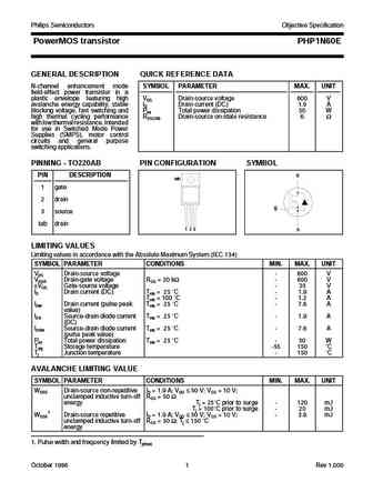
Philips Semiconductors Product specification PowerMOS transistor PHP1N60 GENERAL DESCRIPTION QUICK REFERENCE DATA N-channel enhancement mode SYMBOL PARAMETER MAX. UNIT field-effect power transistor in a plastic envelope featuring high VDS Drain-source voltage 600 V avalanche energy capability, stable ID Drain current (DC) 1.9 A off-state characteristics, fast Ptot Total power dissipati
phx1n60e 1.pdf
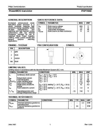
Philips Semiconductors Objective Specification PowerMOS transistor PHX1N60E Isolated version of PHP1N60E GENERAL DESCRIPTION QUICK REFERENCE DATA N-channel enhancement mode SYMBOL PARAMETER MAX. UNIT field-effect power transistor in a full pack, plastic envelope featuring high VDS Drain-source voltage 600 V avalanche energy capability, stable ID Drain current (DC) 1.3 A blocking volt
stf11n60m2-ep.pdf
STF11N60M2-EP Datasheet N-channel 600 V, 0.550 typ., 7.5 A MDmesh M2 EP Power MOSFET in a TO-220FP package Features VDS RDS(on) max. ID Order code STF11N60M2-EP 600 V 0.595 7.5 A Extremely low gate charge Excellent output capacitance (COSS) profile 3 2 1 Very low turn-off switching losses 100% avalanche tested TO-220FP Zener-protected D(2) Applica
tk31n60x.pdf
TK31N60X MOSFETs Silicon N-Channel MOS (DTMOS -H) TK31N60X TK31N60X TK31N60X TK31N60X 1. Applications 1. Applications 1. Applications 1. Applications Switching Voltage Regulators 2. Features 2. Features 2. Features 2. Features (1) Low drain-source on-resistance RDS(ON) = 0.073 (typ.) by used to Super Junction Structure DTMOS (2) High-speed switching properties wit
tk31n60w5.pdf
TK31N60W5 MOSFETs Silicon N-Channel MOS (DTMOS ) TK31N60W5 TK31N60W5 TK31N60W5 TK31N60W5 1. Applications 1. Applications 1. Applications 1. Applications Switching Voltage Regulators 2. Features 2. Features 2. Features 2. Features (1) Fast reverse recovery time trr = 135 ns (typ.) (2) Low drain-source on-resistance RDS(ON) = 0.082 (typ.) by used to Super Junction St
tk31n60w.pdf

TK31N60W MOSFETs Silicon N-Channel MOS (DTMOS ) TK31N60W TK31N60W TK31N60W TK31N60W 1. Applications 1. Applications 1. Applications 1. Applications Switching Voltage Regulators 2. Features 2. Features 2. Features 2. Features (1) Low drain-source on-resistance RDS(ON) = 0.073 (typ.) by used to Super Junction Structure DTMOS (2) Easy to control Gate switching (3) E
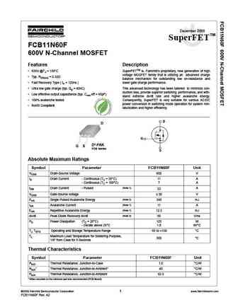
fcb11n60tm.pdf
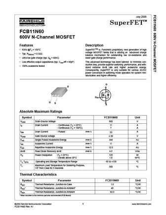
July 2005 TM SuperFET FCB11N60 600V N-Channel MOSFET Features Description 650V @TJ = 150 C SuperFETTM is, Farichild s proprietary, new generation of high voltage MOSFET family that is utilizing an advanced charge Typ. RDS(on) = 0.32 balance mechanism for outstanding low on-resistance and Ultra low gate charge (typ. Qg = 40nC) lower gate charge performance. Low
fqp1n60.pdf
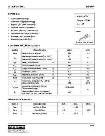
QFET N-CHANNEL FQP1N60 FEATURES BVDSS = 600V Advanced New Design RDS(ON) = 11.5 Avalanche Rugged Technology ID = 1.2A Rugged Gate Oxide Technology Very Low Intrinsic Capacitances Excellent Switching Characteristics TO-220 Unrivalled Gate Charge 5.0nC (Typ.) Extended Safe Operating Area 1 Lower RDS(ON) 9.3 (Typ.) 2 3 1. Gate 2. Drain 3. Sou
fcp11n60n fcpf11n60nt.pdf
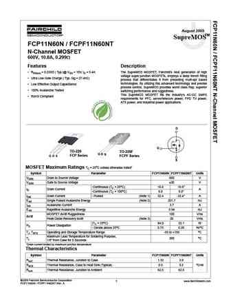
August 2009 SupreMOSTM FCP11N60N / FCPF11N60NT tm N-Channel MOSFET 600V, 10.8A, 0.299 Features Description RDS(on) = 0.255 ( Typ.)@ VGS = 10V, ID = 5.4A The SupreMOS MOSFET, Fairchild s next generation of high voltage super-junction MOSFETs, employs a deep trench filling Ultra Low Gate Charge ( Typ. Qg = 27.4nC) process that differentiates it from preceding multi-epi
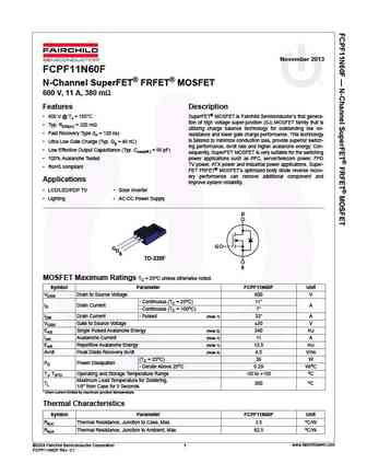
fch041n60f f085.pdf
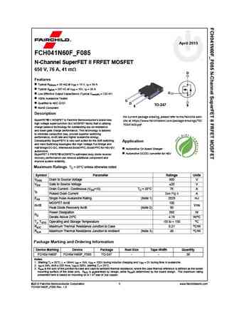
April 2015 FCH041N60F_F085 N-Channel SuperFET II FRFET MOSFET 650 V, 76 A, 41 m D Features Typical RDS(on) = 36 m at VGS = 10 V, ID = 38 A Typical Qg(tot) = 267 nC at VGS = 10V, ID = 38 A G Low Effective Output Capacitance (Typical Coss(eff.) = 720 nF) 100% Avalanche Tested G Qualified to AEC Q101 D TO-247 S S RoHS Compliant Description For current package dra
fcb11n60ftm.pdf
December 2008 TM SuperFET FCB11N60F 600V N-Channel MOSFET Features Description 650V @TJ = 150 C SuperFETTM is, Fairchild s proprietary, new generation of high voltage MOSFET family that is utilizing an advanced charge Typ. RDS(on) = 0.32 balance mechanism for outstanding low on-resistance and Fast Recovery Type ( trr = 120ns ) lower gate charge performance.
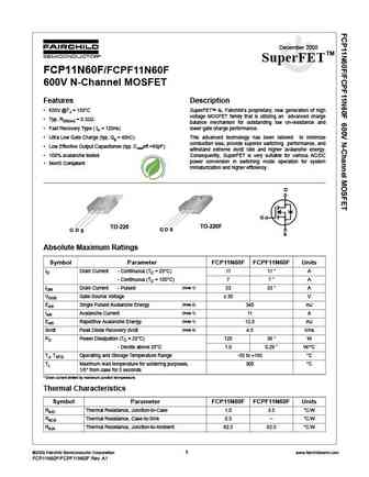
fcp11n60 fcpf11n60 fcpf11n60t.pdf
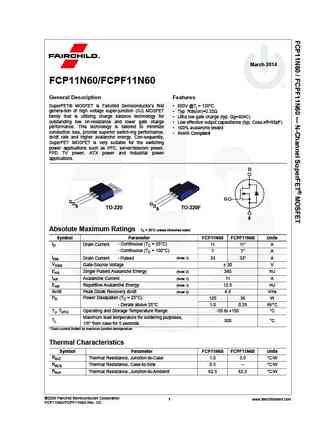
March 2014 FCP11N60/FCPF11N60 General Description Features SuperFET MOSFET is Fairchild Semiconductor s first 650V @Tj = 150 C genera-tion of high voltage super-junction (SJ) MOSFET Typ. Rds(on)=0.32 family that is utilizing charge balance technology for Ultra low gate charge (typ. Qg=40nC) outstanding low on-resistance and lower gate charge Low effective outpu
fcp11n60f fcpf11n60f.pdf
December 2008 TM SuperFET FCP11N60F/FCPF11N60F 600V N-Channel MOSFET Features Description 650V @TJ = 150 C SuperFETTM is, Fairchild s proprietary, new generation of high voltage MOSFET family that is utilizing an advanced charge Typ. RDS(on) = 0.32 balance mechanism for outstanding low on-resistance and Fast Recovery Type ( trr = 120ns) lower gate charge performance
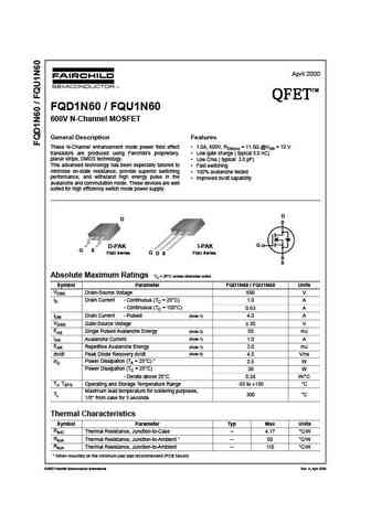
fqd1n60tf fqd1n60tm fqu1n60tu.pdf

April 2000 TM QFET QFET QFET QFET FQD1N60 / FQU1N60 600V N-Channel MOSFET General Description Features These N-Channel enhancement mode power field effect 1.0A, 600V, RDS(on) = 11.5 @VGS = 10 V transistors are produced using Fairchild s proprietary, Low gate charge ( typical 5.0 nC) planar stripe, DMOS technology. Low Crss ( typical 3.0 pF) This advanced technology
fqt1n60c fqt1n60ctf ws.pdf
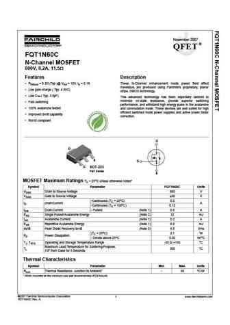
November 2007 QFET FQT1N60C N-Channel MOSFET 600V, 0.2A, 11.5 Features Description RDS(on) = 9.3 (Typ.)@ VGS = 10V, ID = 0.1A These N-Channel enhancement mode power field effect transistors are produced using Fairchild s proprietary, planar Low gate charge ( Typ. 4.8nC) stripe, DMOS technology. Low Crss ( Typ. 3.5pF) This advanced technology has been especia
fch041n60e.pdf
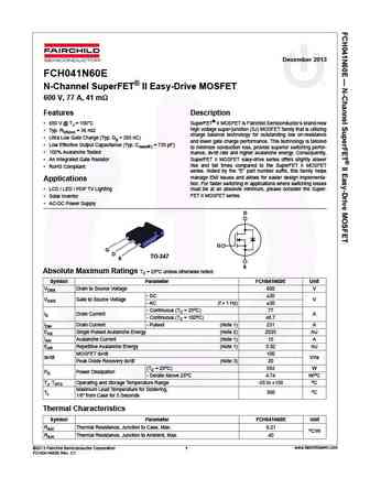
December 2013 FCH041N60E N-Channel SuperFET II Easy-Drive MOSFET 600 V, 77 A, 41 m Features Description 650 V @ TJ = 150 C SuperFET II MOSFET is Fairchild Semiconductor s brand-new high voltage super-junction (SJ) MOSFET family that is utilizing Typ. RDS(on) = 36 m charge balance technology for outstanding low on-resistance Ultra Low Gate Charge (Typ. Qg = 285 nC
fqn1n60cbu fqn1n60cta.pdf

QFET FQN1N60C 600V N-Channel MOSFET Features Description 0.3 A, 600 V, RDS(on) = 11.5 @ VGS = 10 V These N-Channel enhancement mode power field effect transistors are produced using Fairchild s proprietary, planar Low gate charge ( typical 4.8 nC ) stripe, DMOS technology. This advanced technology has been especially tailored to Low Crss ( typical 3.5 pF) minimi
fqb1n60tm.pdf
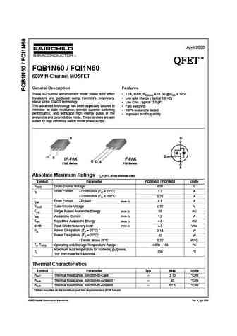
April 2000 TM QFET QFET QFET QFET FQB1N60 / FQI1N60 600V N-Channel MOSFET General Description Features These N-Channel enhancement mode power field effect 1.2A, 600V, RDS(on) = 11.5 @VGS = 10 V transistors are produced using Fairchild s proprietary, Low gate charge ( typical 5.0 nC) planar stripe, DMOS technology. Low Crss ( typical 3.0 pF) This advanced technology
fcpf11n60f.pdf
November 2013 FCPF11N60F N-Channel SuperFET FRFET MOSFET 600 V, 11 A, 380 m Features Description 600 V @ TJ = 150 C SuperFET MOSFET is Fairchild Semiconductor s first genera- tion of high voltage super-junction (SJ) MOSFET family that is Typ. RDS(on) = 320 m utilizing charge balance technology for outstanding low on- Fast Recovery Type (trr = 120 ns) resistanc
fqd1n60 fqu1n60.pdf
April 2000 TM QFET QFET QFET QFET FQD1N60 / FQU1N60 600V N-Channel MOSFET General Description Features These N-Channel enhancement mode power field effect 1.0A, 600V, RDS(on) = 11.5 @VGS = 10 V transistors are produced using Fairchild s proprietary, Low gate charge ( typical 5.0 nC) planar stripe, DMOS technology. Low Crss ( typical 3.0 pF) This advanced technology
fch041n60f.pdf
December 2013 FCH041N60F N-Channel SuperFET II FRFET MOSFET 600 V, 76 A, 41 m Features Description 650 V @ TJ = 150 C SuperFET II MOSFET is Fairchild Semiconductor s brand-new high voltage super-junction (SJ) MOSFET family that is utilizing Typ. RDS(on) = 36 m charge balance technology for outstanding low on-resistance and lower gate charge performance. This techn
fqpf1n60 fqpf1n60t.pdf
April 2000 TM QFET QFET QFET QFET FQPF1N60 600V N-Channel MOSFET General Description Features These N-Channel enhancement mode power field effect 0.9A, 600V, RDS(on) = 11.5 @VGS = 10 V transistors are produced using Fairchild s proprietary, Low gate charge ( typical 5.0 nC) planar stripe, DMOS technology. Low Crss ( typical 3.0 pF) This advanced technology has been
fcp11n60 fcpf11n60.pdf
December 2008 TM SuperFET FCP11N60/FCPF11N60 General Description Features SuperFETTM is a new generation of high voltage MOSFETs 650V @Tj = 150 C from Fairchild with outstanding low on-resistance and low Typ. Rds(on)=0.32 gate charge performance, a result of proprietary technology Ultra low gate charge (typ. Qg=40nC) utilizing advanced charge balance mechanisms. L
fqd1n60ctf fqd1n60ctm fqd1n60c fqu1n60c fqu1n60ctu.pdf
January 2009 QFET FQD1N60C / FQU1N60C 600V N-Channel MOSFET General Description Features These N-Channel enhancement mode power field effect 1A, 600V, RDS(on) = 11.5 @VGS = 10 V transistors are produced using Fairchild s proprietary, Low gate charge ( typical 4.8nC) planar stripe, DMOS technology. Low Crss ( typical 3.5 pF) This advanced technology has been especiall
ssr1n60b ssr1n60btm ssu1n60b.pdf
November 2001 SSR1N60B / SSU1N60B 600V N-Channel MOSFET General Description Features These N-Channel enhancement mode power field effect 0.9A, 600V, RDS(on) = 12 @VGS = 10 V transistors are produced using Fairchild s proprietary, Low gate charge ( typical 5.9 nC) planar, DMOS technology. Low Crss ( typical 3.6 pF) This advanced technology has been especially tailored to
fqn1n60c.pdf
QFET FQN1N60C 600V N-Channel MOSFET Features Description 0.3 A, 600 V, RDS(on) = 11.5 @ VGS = 10 V These N-Channel enhancement mode power field effect transistors are produced using Fairchild s proprietary, planar Low gate charge ( typical 4.8 nC ) stripe, DMOS technology. This advanced technology has been especially tailored to Low Crss ( typical 3.5 pF) minimi
ssw1n60a.pdf
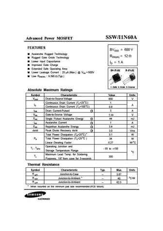
Advanced Power MOSFET FEATURES BVDSS = 600 V Avalanche Rugged Technology RDS(on) = 12 Rugged Gate Oxide Technology Lower Input Capacitance ID = 1 A Improved Gate Charge Extended Safe Operating Area Lower Leakage Current 25 A (Max.) @ VDS = 600V 2 Low RDS(ON) 9.390 (Typ.) 1 1 2 3 3 1. Gate 2. Drain 3. Source Absolute Maximum Ratings Symbol Characte
ssr1n60a.pdf
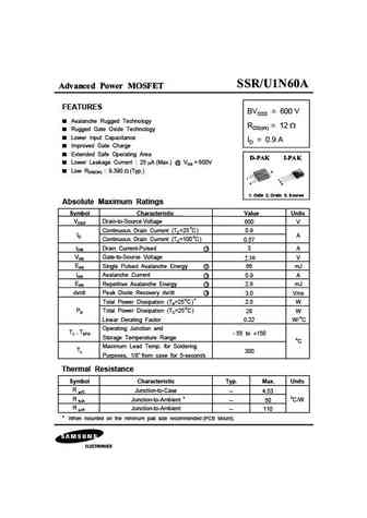
Advanced Power MOSFET FEATURES BVDSS = 600 V Avalanche Rugged Technology RDS(on) = 12 Rugged Gate Oxide Technology Lower Input Capacitance ID = 0.9 A Improved Gate Charge Extended Safe Operating Area Lower Leakage Current 25 A (Max.) @ VDS = 600V Low RDS(ON) 9.390 (Typ.) 2 1 1 2 3 3 1. Gate 2. Drain 3. Source Absolute Maximum Ratings Symbol Charact
ssp1n60a.pdf
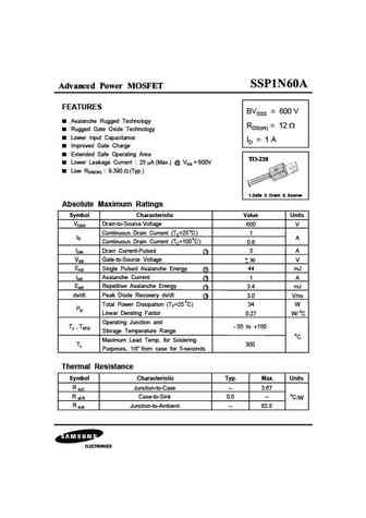
Advanced Power MOSFET FEATURES BVDSS = 600 V Avalanche Rugged Technology RDS(on) = 12 Rugged Gate Oxide Technology Lower Input Capacitance ID = 1 A Improved Gate Charge Extended Safe Operating Area Lower Leakage Current 25 A (Max.) @ VDS = 600V Low RDS(ON) 9.390 (Typ.) 1 2 3 1.Gate 2. Drain 3. Source Absolute Maximum Ratings Symbol Characteristic Value U
irfp21n60l irfp21n60lpbf sihfp21n60l.pdf
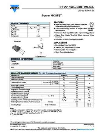
IRFP21N60L, SiHFP21N60L Vishay Siliconix Power MOSFET FEATURES PRODUCT SUMMARY Superfast Body Diode Eliminates the Need for VDS (V) 600 External Diodes in ZVS Applications Available RDS(on) ( )VGS = 10 V 0.27 Lower Gate Charge Results in Simple Drive RoHS* Qg (Max.) (nC) 150 COMPLIANT Requirements Qgs (nC) 46 Enhanced dV/dt Capabilities Offer Improved Ruggedness Qgd
siha21n60ef.pdf
SiHA21N60EF www.vishay.com Vishay Siliconix EF Series Power MOSFET with Fast Body Diode FEATURES D Thin-Lead TO-220 FULLPAK Fast body diode MOSFET using E series technology Reduced trr, Qrr, and IRRM Low figure-of-merit (FOM) Ron x Qg G Low input capacitance (Ciss) Available Increased robustness due to low Qrr Ultra low gate charge (Qg) Avalanche en
irfr1n60a irfu1n60a sihfr1n60a sihfu1n60a.pdf

IRFR1N60A, IRFU1N60A, SiHFR1N60A, SiHFU1N60A Vishay Siliconix Power MOSFET FEATURES PRODUCT SUMMARY Halogen-free According to IEC 61249-2-21 VDS (V) 600 Definition RDS(on) (Max.) ( )VGS = 10 V 7.0 Low Gate Charge Qg Results in Simple Drive Qg (Max.) (nC) 14 Requirement Qgs (nC) 2.7 Improved Gate, Avalanche and Dynamic Qgd (nC) 8.1 dV/dt Ruggedness Configuration Sing
irfu1n60a sihfr1n60a sihfu1n60a.pdf
IRFR1N60A, IRFU1N60A, SiHFR1N60A, SiHFU1N60A Vishay Siliconix Power MOSFET FEATURES PRODUCT SUMMARY Halogen-free According to IEC 61249-2-21 VDS (V) 600 Definition RDS(on) (Max.) ( )VGS = 10 V 7.0 Low Gate Charge Qg Results in Simple Drive Qg (Max.) (nC) 14 Requirement Qgs (nC) 2.7 Improved Gate, Avalanche and Dynamic Qgd (nC) 8.1 dV/dt Ruggedness Configuration Sing
sihh21n60e.pdf
SiHH21N60E www.vishay.com Vishay Siliconix E Series Power MOSFET FEATURES PRODUCT SUMMARY Fully lead (Pb)-free device VDS (V) at TJ max. 650 Low figure-of-merit (FOM) Ron x Qg RDS(on) typ. ( ) at 25 C VGS = 10 V 0.153 Low input capacitance (Ciss) Qg max. (nC) 83 Reduced switching and conduction losses Qgs (nC) 11 Qgd (nC) 20 Ultra low gate charge (Qg) Conf
sihh11n60e.pdf
SiHH11N60E www.vishay.com Vishay Siliconix E Series Power MOSFET FEATURES PRODUCT SUMMARY Fully lead (Pb)-free device VDS (V) at TJ max. 650 Low figure-of-merit (FOM) Ron x Qg RDS(on) typ. ( ) at 25 C VGS = 10 V 0.295 Low input capacitance (Ciss) Qg max. (nC) 62 Reduced switching and conduction losses Qgs (nC) 7 Qgd (nC) 13 Ultra low gate charge (Qg) Confi
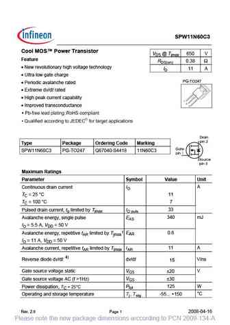
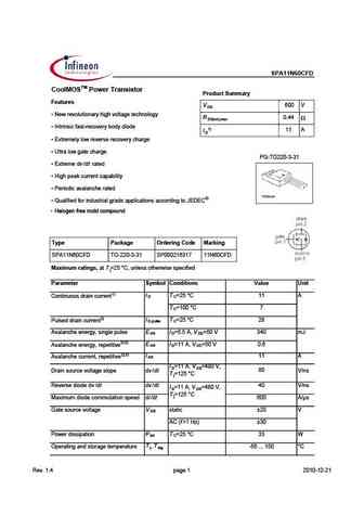
spw11n60cfd.pdf
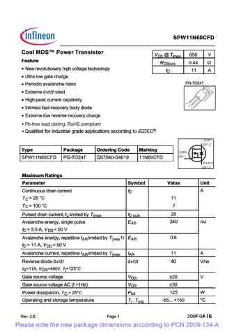
SPW11N60CFD C I MOS P wer TransIst r VDS @ Tjmax 650 V DS Feature RDS(on) 0.44 New revolutionary high voltage technology ID 11 A 11 Ultra low gate charge PG-TO247 Periodic avalanche rated Extreme dv/dt rated /d High peak current capability Intrinsic fast-recovery body diode Extreme low reverse recovery charge 0) Qualified for industrial grade
spp11n60cfd.pdf
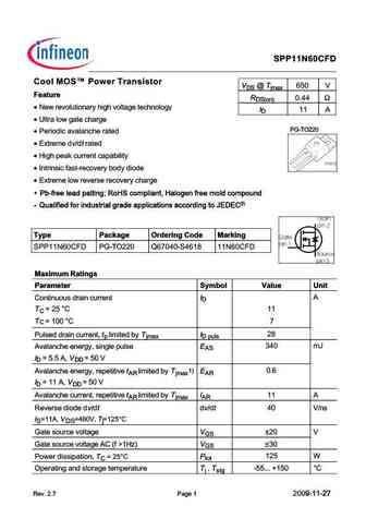
SPP11N60CFD C I MOS P wer Transist r VDS @ Tjmax 650 V Feature RDS(on) 0.44 New revolutionary high voltage technology ID 11 A Ultra low gate charge PG-TO220 Periodic avalanche rated Extreme dv/dt rated High peak current capability Intrinsic fast-recovery body diode Extreme low reverse recovery charge Type Package Ordering C de Marking SPP11N60CF
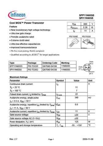
spp11n60c3 spi11n60c3 spa11n60c3 spa11n60c3e8185.pdf
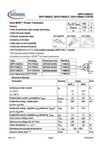
SPP11N60C3 SPI11N60C3, SPA11N60C3, SPA11N60C3 E8185 Cool MOS Power Transistor VDS @ Tjmax 650 V Feature RDS(on) 0.38 New revolutionary high voltage technology ID 11 A Ultra low gate charge PG-TO220FP PG-TO262 PG-TO220 Periodic avalanche rated Extreme dv/dt rated 3 High peak current capability 2 1 P-TO220-3-31 Improved transconductance PG-TO-2
spi11n60cfd.pdf
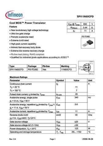
SPI11N60CFD C I MOS P wer Transist r VDS @ Tjmax 650 V Feature RDS(on) 0.44 New revolutionary high voltage technology ID 11 A Ultra low gate charge PG-TO262 Periodic avalanche rated Extreme dv/dt rated High peak current capability Intrinsic fast-recovery body diode Extreme low reverse recovery charge 0) Qualified for industrial grade applications
sps01n60c3.pdf
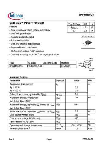
SPS01N60C3 Cool MOS Power Transistor VDS @ Tjmax 650 V Feature RDS(on) 6 New revolutionary high voltage technology ID 0.8 A Ultra low gate charge PG-TO251-3-11 Periodic avalanche rated Extreme dv/dt rated Ultra low effective capacitances Improved transconductance Type Package Ordering Code Marking SPS01N60C3 PG-TO251-3-11 - 01N60C3 Maximum Ratings
spb11n60c3.pdf
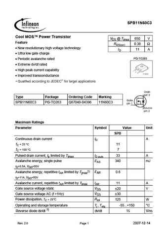
SPB11N60C3 Cool MOS Power Transistor VDS @ Tjmax 650 V Feature RDS(on) 0.38 New revolutionary high voltage technology ID 11 A Ultra low gate charge PG-TO263 Periodic avalanche rated Extreme dv/dt rated High peak current capability Improved transconductance Type Package Ordering Code Marking SPB11N60C3 PG-TO263 Q67040-S4396 11N60C3 Maximum Ratings P
spp11n60c3 spi11n60c3 spa11n60c3 e8185 rev.3.2.pdf
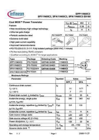
SPP11N60C3 SPI11N60C3, SPA11N60C3, SPA11N60C3 E8185 Cool MOS Power Transistor VDS @ Tjmax 650 V Feature RDS(on) 0.38 New revolutionary high voltage technology ID 11 A Ultra low gate charge PG-TO220FP PG-TO262 PG-TO220 Periodic avalanche rated Extreme dv/dt rated 3 High peak current capability 2 1 P-TO220-3-31 Improved transconductance PG-TO-2
spw11n60s5.pdf
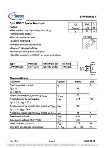
SPW11N60S5 Cool MOS Power Transistor VDS 600 V Feature RDS(on) 0.38 New revolutionary high voltage technology ID 11 A Ultra low gate charge PG-TO247 Periodic avalanche rated Extreme dv/dt rated Ultra low effective capacitances Improved transconductance Type Package Ordering Code Marking SPW11N60S5 PG-TO247 Q67040-S4239 11N60S5 Maximum Ratings Para
spa11n60cfd.pdf
SPA11N60CFD CoolMOSTM Power Transistor Product Summary Features V 600 V DS New revolutionary high voltage technology R 0.44 DS(on),max Intrinsic fast-recovery body diode 1) 11 A I D Extremely low reverse recovery charge Ultra low gate charge PG-TO220-3-31 Extreme dv /dt rated High peak current capability Periodic avalanche rated Qualified for
spb11n60s5.pdf
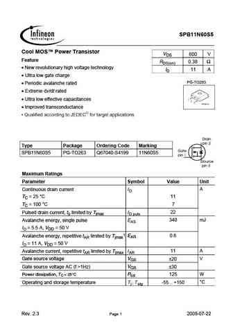
SPB11N60S5 Cool MOS Power Transistor VDS 600 V Feature RDS(on) 0.38 New revolutionary high voltage technology ID 11 A Ultra low gate charge PG-TO263 Periodic avalanche rated Extreme dv/dt rated Ultra low effective capacitances Improved transconductance Type Package Ordering Code Marking 11N60S5 SPB11N60S5 PG-TO263 Q67040-S4199 Maximum Ratings Par
spp11n60s5 spi11n60s5 spp11n60s5 spi11n60s5 .pdf
SPP11N60S5 SPI11N60S5 Cool MOS Power Transistor VDS 600 V Feature RDS(on) 0.38 New revolutionary high voltage technology ID 11 A Ultra low gate charge PG-TO262 PG-TO220 Periodic avalanche rated 2 Extreme dv/dt rated Ultra low effective capacitances 3 2 1 Improved transconductance P-TO220-3-1 Type Package Ordering Code Marking 11N60S5 SPP11N60
ixgt31n60d1.pdf
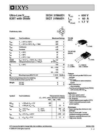
Ultra-Low VCE(sat) IXGH 31N60D1 VCES = 600 V IGBT with Diode IXGT 31N60D1 IC25 = 60 A VCE(sat) = 1.7 V Preliminary data Symbol Test Conditions Maximum Ratings TO-268 (IXGT) VCES TJ = 25 C to 150 C 600 V VCGR TJ = 25 C to 150 C; RGE = 1 MW 600 V G E C (TAB) VGES Continuous 20 V VGEM Transient 30 V TO-247 AD IC25 TC = 25 C60 A (IXGH) IC90 TC = 90 C31 A ICM TC = 25 C, 1
ixgt31n60.pdf

Ultra-Low VCE(sat) IGBT IXGH 31N60 VCES = 600 V IXGT 31N60 IC25 = 60 A VCE(sat) = 1.7 V Symbol Test Conditions Maximum Ratings TO-247 AD VCES TJ = 25 C to 150 C 600 V G VCGR TJ = 25 C to 150 C; RGE = 1 MW 600 V C (TAB) E VGES Continuous 20 V VGEM Transient 30 V IC25 TC = 25 C60 A TO-268 IC90 TC = 90 C31 A ICM TC = 25 C, 1 ms 80 A G SSOA VGE= 15 V, TVJ = 125 C, RG = 1
ixgh41n60.pdf
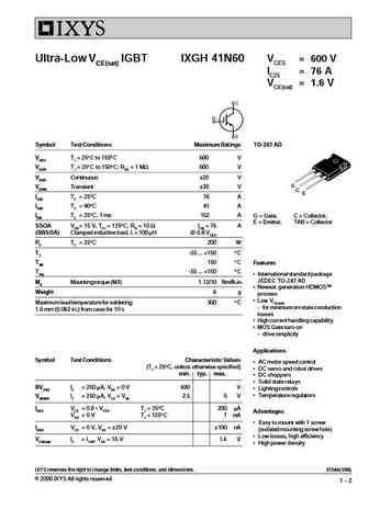
Ultra-Low VCE(sat) IGBT IXGH 41N60 VCES = 600 V IC25 = 76 A VCE(sat) = 1.6 V Symbol Test Conditions Maximum Ratings TO-247 AD VCES TJ = 25 C to 150 C 600 V VCGR TJ = 25 C to 150 C; RGE = 1 MW 600 V VGES Continuous 20 V G VGEM Transient 30 V C E IC25 TC = 25 C76 A IC90 TC = 90 C41 A ICM TC = 25 C, 1 ms 152 A G = Gate, C = Collector, E = Emitter, TAB = Collector SSOA VG
ixgh31n60d1.pdf

Ultra-Low VCE(sat) IXGH 31N60D1 VCES = 600 V IGBT with Diode IXGT 31N60D1 IC25 = 60 A VCE(sat) = 1.7 V Preliminary data Symbol Test Conditions Maximum Ratings TO-268 (IXGT) VCES TJ = 25 C to 150 C 600 V VCGR TJ = 25 C to 150 C; RGE = 1 MW 600 V G E C (TAB) VGES Continuous 20 V VGEM Transient 30 V TO-247 AD IC25 TC = 25 C60 A (IXGH) IC90 TC = 90 C31 A ICM TC = 25 C, 1
ixgh31n60.pdf
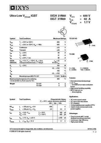
Ultra-Low VCE(sat) IGBT IXGH 31N60 VCES = 600 V IXGT 31N60 IC25 = 60 A VCE(sat) = 1.7 V Symbol Test Conditions Maximum Ratings TO-247 AD VCES TJ = 25 C to 150 C 600 V G VCGR TJ = 25 C to 150 C; RGE = 1 MW 600 V C (TAB) E VGES Continuous 20 V VGEM Transient 30 V IC25 TC = 25 C60 A TO-268 IC90 TC = 90 C31 A ICM TC = 25 C, 1 ms 80 A G SSOA VGE= 15 V, TVJ = 125 C, RG = 1
om11n60sa.pdf
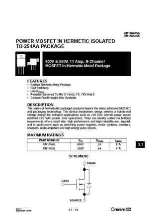
OM11N60SA OM11N55SA POWER MOSFET IN HERMETIC ISOLATED TO-254AA PACKAGE 600V & 550V, 11 Amp, N-Channel MOSFET In Hermetic Metal Package FEATURES Isolated Hermetic Metal Package Fast Switching Low RDS(on) Available Screened To MIL-S-19500, TX, TXV And S Ceramic Feedthroughs Also Available DESCRIPTION This series of hermetically packaged products feature the latest
fcp11n60n fcpf11n60nt.pdf

Is Now Part of To learn more about ON Semiconductor, please visit our website at www.onsemi.com Please note As part of the Fairchild Semiconductor integration, some of the Fairchild orderable part numbers will need to change in order to meet ON Semiconductor s system requirements. Since the ON Semiconductor product management systems do not have the ability to manage part nomenclatur
fqt1n60c.pdf

Is Now Part of To learn more about ON Semiconductor, please visit our website at www.onsemi.com Please note As part of the Fairchild Semiconductor integration, some of the Fairchild orderable part numbers will need to change in order to meet ON Semiconductor s system requirements. Since the ON Semiconductor product management systems do not have the ability to manage part nomenclatur
fqd1n60c fqu1n60c.pdf

Is Now Part of To learn more about ON Semiconductor, please visit our website at www.onsemi.com Please note As part of the Fairchild Semiconductor integration, some of the Fairchild orderable part numbers will need to change in order to meet ON Semiconductor s system requirements. Since the ON Semiconductor product management systems do not have the ability to manage part nomenclatur
nddl01n60z.pdf
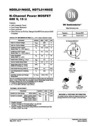
NDDL01N60Z, NDTL01N60Z N-Channel Power MOSFET 600 V, 15 W Features 100% Avalanche Tested Gate Charge Minimized http //onsemi.com Zener-protected These Devices are Pb-Free, Halogen Free/BFR Free and are RoHS V(BR)DSS RDS(ON) MAX Compliant 600 V 15 W @ 10 V ABSOLUTE MAXIMUM RATINGS (TJ = 25 C unless otherwise noted) Parameter Symbol NDD NDT Unit N-Channel MOSFET Dr
ndd01n60 ndt01n60.pdf
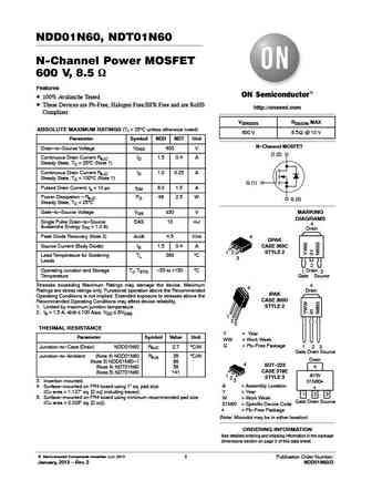
NDD01N60, NDT01N60 N-Channel Power MOSFET 600 V, 8.5 W Features 100% Avalanche Tested These Devices are Pb-Free, Halogen Free/BFR Free and are RoHS http //onsemi.com Compliant V(BR)DSS RDS(ON) MAX ABSOLUTE MAXIMUM RATINGS (TJ = 25 C unless otherwise noted) 600 V 8.5 W @ 10 V Parameter Symbol NDD NDT Unit N-Channel MOSFET Drain-to-Source Voltage VDSS 600 V D (2) Continuou
fch041n60f.pdf

Is Now Part of To learn more about ON Semiconductor, please visit our website at www.onsemi.com Please note As part of the Fairchild Semiconductor integration, some of the Fairchild orderable part numbers will need to change in order to meet ON Semiconductor s system requirements. Since the ON Semiconductor product management systems do not have the ability to manage part nomenclatur
fcp11n60f.pdf

Is Now Part of To learn more about ON Semiconductor, please visit our website at www.onsemi.com Please note As part of the Fairchild Semiconductor integration, some of the Fairchild orderable part numbers will need to change in order to meet ON Semiconductor s system requirements. Since the ON Semiconductor product management systems do not have the ability to manage part nomenclatur
fqn1n60c.pdf

Is Now Part of To learn more about ON Semiconductor, please visit our website at www.onsemi.com Please note As part of the Fairchild Semiconductor integration, some of the Fairchild orderable part numbers will need to change in order to meet ON Semiconductor s system requirements. Since the ON Semiconductor product management systems do not have the ability to manage part nomenclatur
1n60l-tms2-t 1n60g-tms2-t 1n60l-tms4-t 1n60g-tms4-t 1n60l-tn3-r 1n60g-tn3-r 1n60l-tnd-r 1n60g-tnd-r.pdf

UNISONIC TECHNOLOGIES CO., LTD 1N60 Power MOSFET 1.2A, 600V N-CHANNEL POWER MOSFET DESCRIPTION The UTC 1N60 is a high voltage MOSFET and is designed to have better characteristics, such as fast switching time, low gate charge, low on-state resistance and have a high rugged avalanche characteristics. This power MOSFET is usually used at high speed switching applications in
1n60g-aa3-r 1n60l-ta3-t 1n60g-ta3-t 1n60l-tf2-t 1n60g-tf2-t 1n60l-tf3-t 1n60g-tf3-t 1n60l-tm3-t 1n60g-tm3-t.pdf

UNISONIC TECHNOLOGIES CO., LTD 1N60 Power MOSFET 1.2A, 600V N-CHANNEL POWER MOSFET DESCRIPTION The UTC 1N60 is a high voltage MOSFET and is designed to have better characteristics, such as fast switching time, low gate charge, low on-state resistance and have a high rugged avalanche characteristics. This power MOSFET is usually used at high speed switching applications in
1n60l-t92-b 1n60g-t92-b 1n60l-t92-k 1n60g-t92-k 1n60l-tms-t 1n60g-tms-t 1n60l-t60-k 1n60g-t60-k.pdf

UNISONIC TECHNOLOGIES CO., LTD 1N60 Power MOSFET 1.2A, 600V N-CHANNEL POWER MOSFET DESCRIPTION The UTC 1N60 is a high voltage MOSFET and is designed to have better characteristics, such as fast switching time, low gate charge, low on-state resistance and have a high rugged avalanche characteristics. This power MOSFET is usually used at high speed switching applications in
1n60z.pdf
UNISONIC TECHNOLOGIES CO., LTD 1N60Z Power MOSFET 1.2A, 600V N-CHANNEL POWER MOSFET DESCRIPTION The UTC 1N60Z is a high voltage MOSFET and is designed to have better characteristics, such as fast switching time, low gate charge, low on-state resistance and high rugged avalanche characteristics. This power MOSFET is usually used at high speed switching applications in power s
1n60l-aa3-r 1n60g-aa3-r 1n60l-ab3-r 1n60g-ab3-r 1n60l-tm3-t 1n60g-tm3-t 1n60l-tn3-r 1n60g-tn3-r 1n60l-t60-k 1n60g-t60-k 1n60l-t92-b 1n60g-t92-b 1n60l-t92-k 1n60g-t92-k.pdf
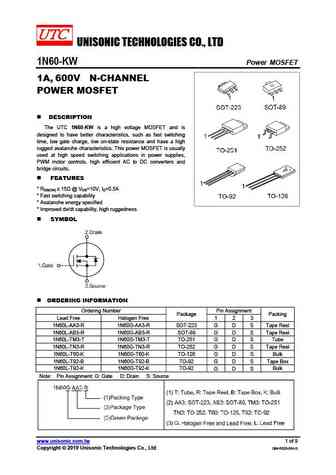
UNISONIC TECHNOLOGIES CO., LTD 1N60-KW Power MOSFET 1A, 600V N-CHANNEL POWER MOSFET DESCRIPTION The UTC 1N60-KW is a high voltage MOSFET and is designed to have better characteristics, such as fast switching time, low gate charge, low on-state resistance and have a high rugged avalanche characteristics. This power MOSFET is usually used at high speed switching applications
1n60a.pdf
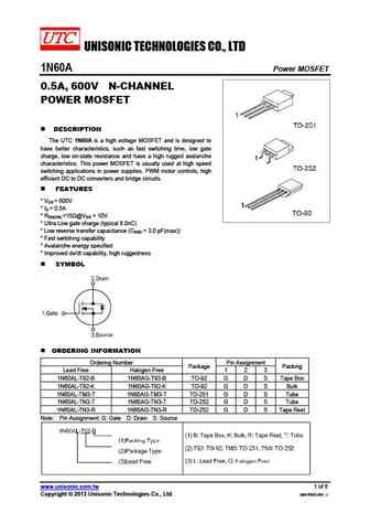
UNISONIC TECHNOLOGIES CO., LTD 1N60A Power MOSFET 0.5A, 600V N-CHANNEL POWER MOSFET DESCRIPTION The UTC 1N60A is a high voltage MOSFET and is designed to have better characteristics, such as fast switching time, low gate charge, low on-state resistance and have a high rugged avalanche characteristics. This power MOSFET is usually used at high speed switching applications i
1n60p.pdf
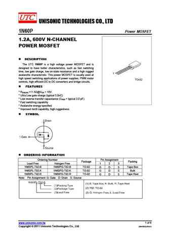
UNISONIC TECHNOLOGIES CO., LTD 1N60P Power MOSFET 1.2A, 600V N-CHANNEL POWER MOSFET DESCRIPTION The UTC 1N60P is a high voltage power MOSFET and is designed to have better characteristics, such as fast switching time, low gate charge, low on-state resistance and a high rugged avalanche characteristic. This power MOSFET is usually used at high speed switching applications of
1n60l-tms2-t 1n60g-tms2-t 1n60l-tms4-t 1n60g-tms4-t 1n60l-tn3-r 1n60g-tn3-r 1n60l-tnd-r 1n60g-tnd-r 1n60l-t60-k 1n60g-t60-k 1n60l-t92-b 1n60g-t92-b 1n60l-t92-k.pdf

UNISONIC TECHNOLOGIES CO., LTD 1N60 Power MOSFET 1.2A, 600V N-CHANNEL POWER MOSFET DESCRIPTION The UTC 1N60 is a high voltage MOSFET and is designed to have better characteristics, such as fast switching time, low gate charge, low on-state resistance and have a high rugged avalanche characteristics. This power MOSFET is usually used at high speed switching applications in
1n60l-aa3-r 1n60g-aa3-r 1n60l-ta3-t 1n60g-ta3-t 1n60l-tf2-t 1n60g-tf2-t 1n60l-tf3-t 1n60g-tf3-t 1n60l-tm3-t 1n60g-tm3-t 1n60l-tms-t 1n60g-tms-t 1n60g-t92-k.pdf
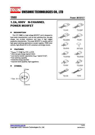
UNISONIC TECHNOLOGIES CO., LTD 1N60 Power MOSFET 1.2A, 600V N-CHANNEL POWER MOSFET DESCRIPTION The UTC 1N60 is a high voltage MOSFET and is designed to have better characteristics, such as fast switching time, low gate charge, low on-state resistance and have a high rugged avalanche characteristics. This power MOSFET is usually used at high speed switching applications in
apt31n60bcsg apt31n60scsg.pdf
FINAL DATA SHEET 600V 31A 0.100 APT31N60BCS APT31N60SCS APT31N60BCSG* APT31N60SCSG* *G Denotes RoHS Compliant, Pb Free Terminal Finish. Super Junction MOSFET (B) COOLMOS Power Semiconductors D3PAK Ultra Low RDS(ON) (S) Low Miller Capacitance Ultra Low Gate Charge, Qg D Avalanche Energy Rated Extreme dv/dt Rated G Popular TO-247 or Surface M
fmv11n60e.pdf
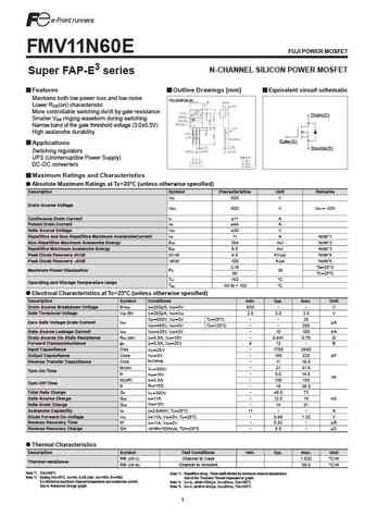
FMV11N60E FUJI POWER MOSFET N-CHANNEL SILICON POWER MOSFET Super FAP-E3 series Features Outline Drawings [mm] Equivalent circuit schematic Maintains both low power loss and low noise TO-220F(SLS) Lower R (on) characteristic DS More controllable switching dv/dt by gate resistance Drain(D) Smaller V ringing waveform during switching GS Narrow band of the gate threshold voltage (3.0 0
fmi11n60e.pdf
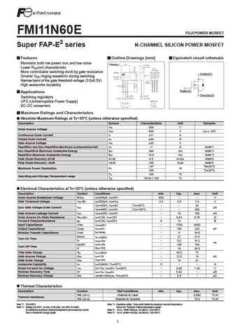
FMI11N60E FUJI POWER MOSFET Super FAP-E3 series N-CHANNEL SILICON POWER MOSFET Features Outline Drawings [mm] Equivalent circuit schematic Maintains both low power loss and low noise T-Pack(L) Lower R (on) characteristic DS More controllable switching dv/dt by gate resistance Drain(D) Smaller V ringing waveform during switching GS Narrow band of the gate threshold voltage (3.0 0.5V)
fmc11n60e.pdf
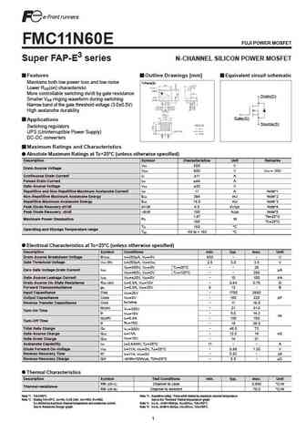
FMC11N60E FUJI POWER MOSFET Super FAP-E3 series N-CHANNEL SILICON POWER MOSFET Features Outline Drawings [mm] Equivalent circuit schematic Maintains both low power loss and low noise T-Pack(S) Lower R (on) characteristic DS More controllable switching dv/dt by gate resistance Drain(D) Smaller V ringing waveform during switching GS Narrow band of the gate threshold voltage (3.0 0.5V)
fmp11n60e.pdf
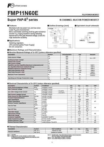
FMP11N60E FUJI POWER MOSFET Super FAP-E3 series N-CHANNEL SILICON POWER MOSFET Features Outline Drawings [mm] Equivalent circuit schematic Maintains both low power loss and low noise TO-220AB Lower R (on) characteristic DS More controllable switching dv/dt by gate resistance Drain(D) Smaller V ringing waveform during switching GS Narrow band of the gate threshold voltage (3.0 0.5V)
sjv01n60.pdf
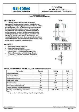
SJV01N60 1A , 600V , RDS(ON) 10 m N-Channel Enhancement Mode Power MOSFET Elektronische Bauelemente RoHS Compliant Product A suffix of -C specifies halogen & lead-free TO-92 DESCRIPTION The high voltage MOSFET uses an advanced A D termination scheme to provide enhanced voltage-blocking capability without degrading performance over time. In addition
tsm1n60s a07.pdf
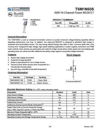
TSM1N60S 600V N-Channel Power MOSFET TO-92 Pin Definition PRODUCT SUMMARY 1. Gate VDS (V) RDS(on)( ) ID (A) 2. Drain 3. Source 600 11 @ VGS =10V 0.3 General Description The TSM1N60S is used an advanced termination scheme to provide enhanced voltage-blocking capability without degrading performance over time. In addition, this advanced MOSFET is designed to withstand
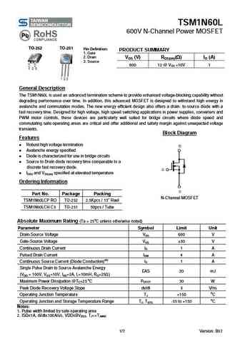
tsm1n60l a07.pdf
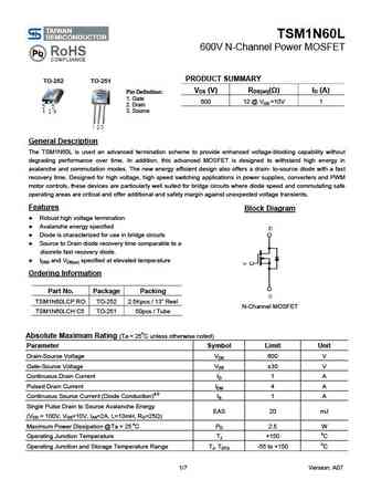
TSM1N60L 600V N-Channel Power MOSFET PRODUCT SUMMARY TO-252 TO-251 VDS (V) RDS(on)( ) ID (A) Pin Definition 1. Gate 600 12 @ VGS =10V 1 2. Drain 3. Source General Description The TSM1N60L is used an advanced termination scheme to provide enhanced voltage-blocking capability without degrading performance over time. In addition, this advanced MOSFET is designed to withs
tsm1n60lch tsm1n60lcp.pdf
TSM1N60L 600V N-Channel Power MOSFET TO-252 TO-251 Pin Definition PRODUCT SUMMARY 1. Gate 2. Drain VDS (V) RDS(on)( ) ID (A) 3. Source 600 12 @ VGS =10V 1 General Description The TSM1N60L is used an advanced termination scheme to provide enhanced voltage-blocking capability without degrading performance over time. In addition, this advanced MOSFET is designed to wit
tsm1n60sct.pdf

TSM1N60S 600V N-Channel Power MOSFET TO-92 Pin Definition PRODUCT SUMMARY 1. Gate VDS (V) RDS(on)( ) ID (A) 2. Drain 3. Source 600 11 @ VGS =10V 0.3 General Description The TSM1N60S is used an advanced termination scheme to provide enhanced voltage-blocking capability without degrading performance over time. In addition, this advanced MOSFET is designed to withstand
cju01n60.pdf
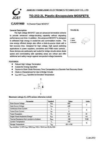
JIANGSU CHANGJIANG ELECTRONICS TECHNOLOGY CO., LTD TO-252-2L Plastic-Encapsulate MOSFETS CJU01N60 N-Channel Power MOSFET TO-252-2L General Description The high voltage MOSFET uses an advanced termination scheme to provide enhanced voltage-blocking capability without degrading performance over time. In addition , this advanced MOSFET is designed 1. GATE 2. DRAIN to withstan
cjd01n60.pdf
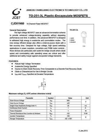
JIANGSU CHANGJIANG ELECTRONICS TECHNOLOGY CO., LTD TO-251-3L Plastic-Encapsulate MOSFETS CJD01N60 N-Channel Power MOSFET TO-251-3L General Description The high voltage MOSFET uses an advanced termination scheme to provide enhanced voltage-blocking capability without degrading performance over time. In addition , this advanced MOSFET is designed 1. GATE 2. DRAIN to withsta
cjv01n60.pdf
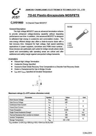
JIANGSU CHANGJIANG ELECTRONICS TECHNOLOGY CO., LTD TO-92 Plastic-Encapsulate MOSFETS CJV01N60 N-Channel Power MOSFET TO-92 General Description The high voltage MOSFET uses an advanced termination scheme to provide enhanced voltage-blocking capability without degrading performance over time. In addition , this advanced MOSFET is designed to withstand high energy in avalanche and
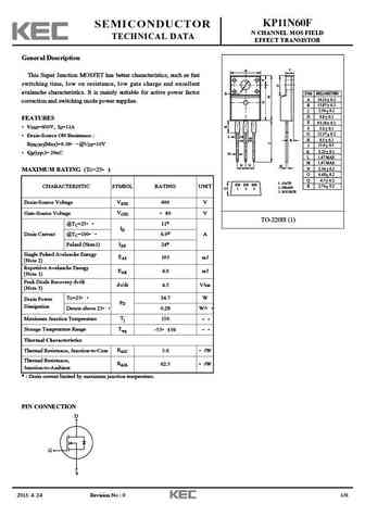
kp11n60f.pdf
KP11N60F SEMICONDUCTOR N CHANNEL MOS FIELD TECHNICAL DATA EFFECT TRANSISTOR General Description C A This Super Junction MOSFET has better characteristics, such as fast switching time, low on resistance, low gate charge and excellent avalanche characteristics. It is mainly suitable for active power factor E DIM MILLIMETERS _ A 10.16 0.2 + correction and switching mode power suppl
kf1n60d-i.pdf
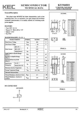
KF1N60D/I SEMICONDUCTOR N CHANNEL MOS FIELD TECHNICAL DATA EFFECT TRANSISTOR General Description KF1N60D This planar stripe MOSFET has better characteristics, such as fast switching time, low on resistance, low gate charge and excellent A K DIM MILLIMETERS avalanche characteristics. It is mainly suitable for switching mode L C D _ A 6.60 + 0.20 _ B 6.10 + 0.20 power supplies.
kf1n60l.pdf
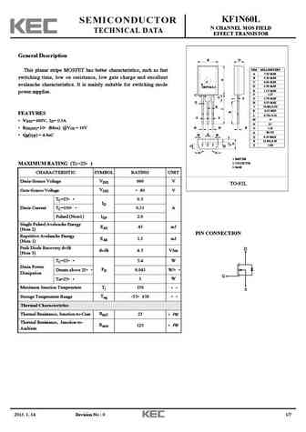
KF1N60L SEMICONDUCTOR N CHANNEL MOS FIELD TECHNICAL DATA EFFECT TRANSISTOR General Description B D DIM MILLIMETERS This planar stripe MOSFET has better characteristics, such as fast A 7.20 MAX switching time, low on resistance, low gate charge and excellent B 5.20 MAX C 0.60 MAX avalanche characteristics. It is mainly suitable for switching mode P D 2.50 MAX DEPTH 0.2 E 1.15 MAX
kp11n60d.pdf
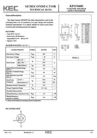
KP11N60D SEMICONDUCTOR N CHANNEL MOS FIELD TECHNICAL DATA EFFECT TRANSISTOR General Description This Super Junction MOSFET has better characteristics, such as fast switching time, low on resistance, low gate charge and excellent A K DIM MILLIMETERS L avalanche characteristics. It is mainly suitable for active power factor C D _ A 6.60 + 0.20 _ B 6.10 + 0.20 correction and swit
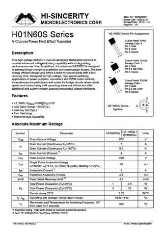
h01n60s.pdf
Spec. No. MOS200501 HI-SINCERITY Issued Date 2005.01.01 Revised Date 2010.11.10 MICROELECTRONICS CORP. Page No. 1/6 H01N60S Series Pin Assignment H01N60S Series 3-Lead Plastic TO-92 N-Channel Power Field Effect Transistor Package Code A Pin 1 Gate Pin 2 Drain Pin 3 Source Description 3 1 2 This high voltage MOSFET uses an advanced termination scheme
h01n60.pdf
Spec. No. MOS200502 HI-SINCERITY Issued Date 2005.03.01 Revised Date 2006.08.31 MICROELECTRONICS CORP. Page No. 1/5 H01N60 Series Pin Assignment H01N60 Series N-Channel Power Field Effect Transistor Tab 3-Lead Plastic TO-252 Package Code J Pin 1 Gate 3 Pin 2 & Tab Drain 2 Description 1 Pin 3 Source This high voltage MOSFET uses an advanced termination scheme to pr
aob11n60.pdf
AOB11N60 600V,11A N-Channel MOSFET General Description Product Summary VDS The AOB11N60 has been fabricated using an advanced 700V@150 high voltage MOSFET process that is designed to deliver ID (at VGS=10V) 11A high levels of performance and robustness in popular AC- RDS(ON) (at VGS=10V)
aou1n60.pdf

AOD1N60/AOU1N60/AOI1N60 600V,1.3A N-Channel MOSFET General Description Product Summary The AOD1N60 & AOU1N60 & AOI1N60 have been fabricated using an advanced high voltage MOSFET VDS 700V@150 process that is designed to deliver high levels of ID (at VGS=10V) 1.3A performance and robustness in popular AC-DC RDS(ON) (at VGS=10V)
aoi1n60l.pdf

AOD1N60/AOU1N60/AOI1N60 600V,1.3A N-Channel MOSFET General Description Product Summary The AOD1N60 & AOU1N60 & AOI1N60 have been fabricated using an advanced high voltage MOSFET VDS 700V@150 process that is designed to deliver high levels of ID (at VGS=10V) 1.3A performance and robustness in popular AC-DC RDS(ON) (at VGS=10V)
aowf11n60.pdf
AOWF11N60 600V,11A N-Channel MOSFET General Description Product Summary VDS The AOWF11N60 has been fabricated using an 700V@150 advanced high voltage MOSFET process that is designed ID (at VGS=10V) 11A to deliver high levels of performance and robustness in RDS(ON) (at VGS=10V)
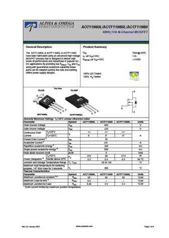
aotf11n60.pdf

AOT11N60/AOTF11N60 600V,11A N-Channel MOSFET General Description Product Summary VDS The AOT11N60 & AOTF11N60 have been fabricated 700V@150 using an advanced high voltage MOSFET process that is ID (at VGS=10V) 11A designed to deliver high levels of performance and RDS(ON) (at VGS=10V)
aot1n60.pdf
AOT1N60 600V,1.3A N-Channel MOSFET General Description Product Summary VDS 700V@150 The AOT1N60 have been fabricated using an advanced high voltage MOSFET process that is designed to deliver ID (at VGS=10V) 1.3A high levels of performance and robustness in popular AC- RDS(ON) (at VGS=10V)
aot11n60.pdf
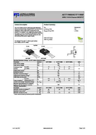
AOT11N60/AOTF11N60 600V,11A N-Channel MOSFET General Description Product Summary VDS The AOT11N60 & AOTF11N60 have been fabricated 700V@150 using an advanced high voltage MOSFET process that is ID (at VGS=10V) 11A designed to deliver high levels of performance and RDS(ON) (at VGS=10V)
aoi1n60.pdf

AOD1N60/AOU1N60/AOI1N60 600V,1.3A N-Channel MOSFET General Description Product Summary The AOD1N60 & AOU1N60 & AOI1N60 have been fabricated using an advanced high voltage MOSFET VDS 700V@150 process that is designed to deliver high levels of ID (at VGS=10V) 1.3A performance and robustness in popular AC-DC RDS(ON) (at VGS=10V)
aod1n60 aou1n60 aoi1n60.pdf
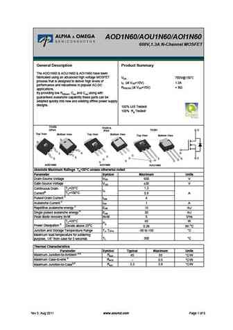
AOD1N60/AOU1N60/AOI1N60 600V,1.3A N-Channel MOSFET General Description Product Summary The AOD1N60 & AOU1N60 & AOI1N60 have been fabricated using an advanced high voltage MOSFET VDS 700V@150 process that is designed to deliver high levels of ID (at VGS=10V) 1.3A performance and robustness in popular AC-DC RDS(ON) (at VGS=10V)
aot11n60l aotf11n60l aotf11n60.pdf
AOT11N60L/AOTF11N60L/AOTF11N60 600V,11A N-Channel MOSFET General Description Product Summary VDS The AOT11N60L & AOTF11N60L & AOTF11N60 700V@150 have been fabricated using an advanced high voltage ID (at VGS=10V) 11A MOSFET process that is designed to deliver high RDS(ON) (at VGS=10V)
aod1n60.pdf

AOD1N60/AOU1N60/AOI1N60 600V,1.3A N-Channel MOSFET General Description Product Summary The AOD1N60 & AOU1N60 & AOI1N60 have been fabricated using an advanced high voltage MOSFET VDS 700V@150 process that is designed to deliver high levels of ID (at VGS=10V) 1.3A performance and robustness in popular AC-DC RDS(ON) (at VGS=10V)
aow11n60.pdf
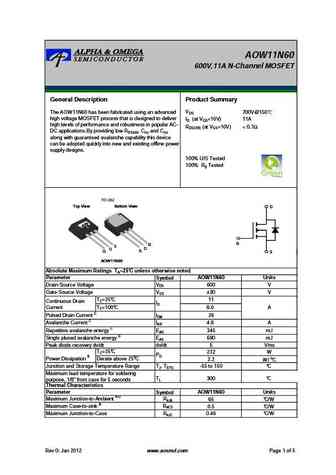
AOW11N60 600V,11A N-Channel MOSFET General Description Product Summary VDS The AOW11N60 has been fabricated using an advanced 700V@150 high voltage MOSFET process that is designed to deliver ID (at VGS=10V) 11A high levels of performance and robustness in popular AC- RDS(ON) (at VGS=10V)
ap01n60hj-hf.pdf
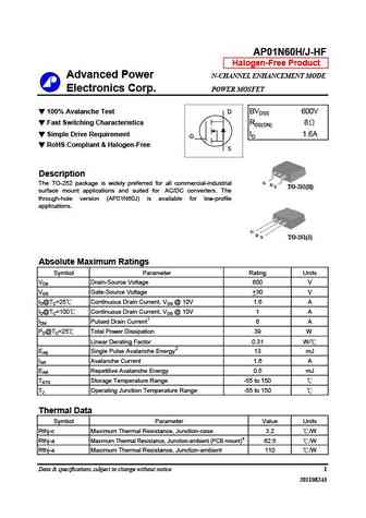
AP01N60H/J-HF Halogen-Free Product Advanced Power N-CHANNEL ENHANCEMENT MODE Electronics Corp. POWER MOSFET 100% Avalanche Test BVDSS 600V D Fast Switching Characteristics RDS(ON) 8 Simple Drive Requirement ID 1.6A G RoHS Compliant & Halogen-Free S Description G The TO-252 package is widely preferred for all commercial-industrial D S TO-252(H) surface mount ap
ap01n60p.pdf
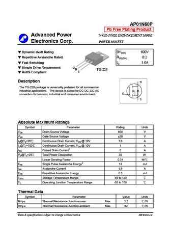
AP01N60P Pb Free Plating Product Advanced Power N-CHANNEL ENHANCEMENT MODE Electronics Corp. POWER MOSFET Dynamic dv/dt Rating BVDSS 600V Repetitive Avalanche Rated RDS(ON) 8 Fast Switching ID 1.6A Simple Drive Requirement G D TO-220 S RoHS Compliant Description D The TO-220 package is universally preferred for all commercial- industrial applications. The de
ap01n60j.pdf
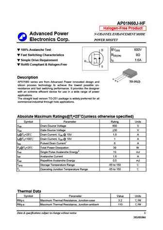
AP01N60J-HF Halogen-Free Product Advanced Power N-CHANNEL ENHANCEMENT MODE Electronics Corp. POWER MOSFET 100% Avalanche Test BVDSS 600V D Fast Switching Characteristics RDS(ON) 8 Simple Drive Requirement ID 1.6A G RoHS Compliant & Halogen-Free S Description G D S TO-251(J) AP01N60 series are from Advanced Power innovated design and silicon process technology
sss1n60.pdf
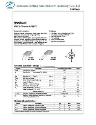
Shenzhen Tuofeng Semiconductor Technology Co., Ltd SSS1N60 SSS1N60 600V N-Channel MOSFET General Description Features These N-Channel enhancement mode power field effect 1.0A, 600V, RDS(on) = 8.5 @VGS = 10 V transistors are produced using proprietary, Low gate charge ( typical 5.9 nC) planar, DMOS technology. Low Crss ( typical 3.6 pF) This advanced technology has been
sif1n60c.pdf
Shenzhen SI Semiconductors Co., LTD. Product Specification Shenzhen SI Semiconductors Co., LTD. Product Specification Shenzhen SI Semiconductors Co., LTD. Product Specification Shenzhen SI Semiconductors Co., LTD. Product Specification N- MOS / N-CHANNEL POWER MOSFET SIF1N60C N- MOS / N-CHANNEL POWER MOSFET SIF1N60C N- MOS / N-CHANN
mtn1n60a3.pdf
Spec. No. C721A3 Issued Date 2010.10.18 CYStech Electronics Corp. Revised Date Page No. 1/10 N-Channel Enhancement Mode Power MOSFET BVDSS 600V RDS(ON) 8 (typ.) MTN1N60A3 ID 1A Description The MTN1N60A3 is a N-channel enhancement-mode MOSFET, providing the designer with the best combination of fast switching, ruggedized device design, low on-resistance and
mtn1n60l3.pdf
Spec. No. C721L3 Issued Date 2014.11.27 CYStech Electronics Corp. Revised Date Page No. 1/9 N-Channel Enhancement Mode Power MOSFET BVDSS 600V MTN1N60L3 ID@VGS=10V, TA=25 C 0.4A ID@VGS=10V, TC=25 C 0.9A RDSON@VGS=10V, ID=0.2A 7.8 (typ) Description The MTN1N60L3 is a N-channel enhancement-mode MOSFET, providing the designer with the best combination of fast sw
cs1n60 to-252.pdf
ShenZhen CanSheng Industry Development Co.,Ltd ShenZhen CanSheng Industry Development Co.,Ltd ShenZhen CanSheng Industry Development Co.,Ltd www.szcansheng.com ShenZhen CanSheng Industry Development Co.,Ltd. TO-252 Plastic-Encapsulate Transistors TO-252 Plastic-Encapsulate Transistors TO-252 Plastic-Encapsulate Transistors TO-252 Plastic-Encapsula
cs1n60 to-92.pdf
ShenZhen CanSheng Industry Development Co.,Ltd. www.szcansheng.com TO-92 Plastic-Encapsulate Transistors 1N60 MOSFET(N-Channel) FEATURES Robust High Voltage Terminrtion Avalanche Energy Specified Source-to-Drain Diode Recovery Time Comparable to a Discrete Fast Recovery Diode Diode is Characterrized for Use in Bridge Circuits MAXIMU
ftu01n60c.pdf
FTU01N60C N-Channel MOSFET Pb Lead Free Package and Finish Applications VDSS RDS(ON) (Max.) ID Adaptor Charger 600V 8.0 1.1A SMPS Features RoHS Compliant D Low ON Resistance Low Gate Charge Peak Current vs Pulse Width Curve Inductive Switching Curves G G D S Ordering Information PART NUMBER PACKAGE BRAND S TO-251 Not to Scale FTU01N
fsn01n60a.pdf
FSN01N60A N-Channel MOSFET Pb Lead Free Package and Finish Applications VDSS RDS(ON) (Typ.) ID Adaptor TV Main Power 600 V 7.0 1.5 A SMPS Power Supply LCD Panel Power Features RoHS Compliant Low ON Resistance Low Gate Charge ESD improved Capability G DS TO-92 Ordering Information PART NUMBER PACKAGE BRAND Packages FSN01N60A TO-92 01N60A
brd1n60.pdf
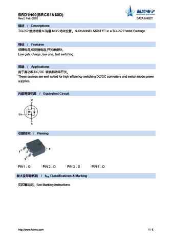
BRD1N60(BRCS1N60D) Rev.C Feb.-2015 DATA SHEET / Descriptions TO-252 N MOS N-CHANNEL MOSFET in a TO-252 Plastic Package. / Features , , Low gate charge, low crss, fast switching. / Applications DC/DC These devices are well suited for high
brf1n60.pdf
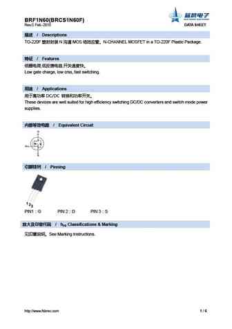
BRF1N60(BRCS1N60F) Rev.C Feb.-2015 DATA SHEET / Descriptions TO-220F N MOS N-CHANNEL MOSFET in a TO-220F Plastic Package. / Features , , Low gate charge, low crss, fast switching. / Applications DC/DC These devices are well suited for hi
br1n60.pdf
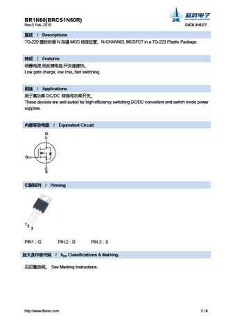
BR1N60(BRCS1N60R) Rev.C Feb.-2015 DATA SHEET / Descriptions TO-220 N MOS N-CHANNEL MOSFET in a TO-220 Plastic Package. / Features , , Low gate charge, low crss, fast switching. / Applications DC/DC These devices are well suited for high
bri1n60.pdf
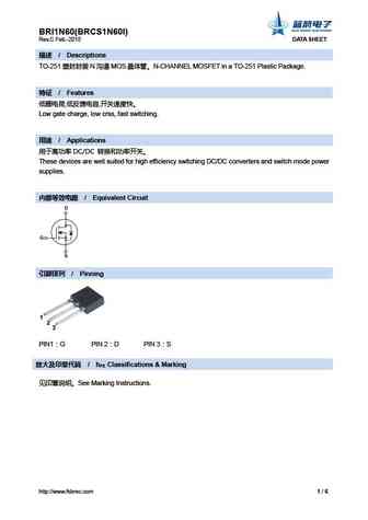
BRI1N60(BRCS1N60I) Rev.C Feb.-2015 DATA SHEET / Descriptions TO-251 N MOS N-CHANNEL MOSFET in a TO-251 Plastic Package. / Features , , Low gate charge, low crss, fast switching. / Applications DC/DC These devices are well suited for high ef
brs1n60.pdf
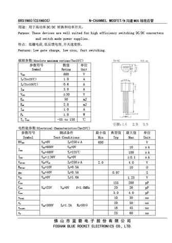
BRS1N60(CS1N60S) N-CHANNEL MOSFET/N MOS DC/DC Purpose These devices are well suited for high efficiency switching DC/DC converters and switch mode power supplies. , , Features Low gate charge, low crss, fast switching. /Absolute maximum ratings(Ta=25
l1n60.pdf
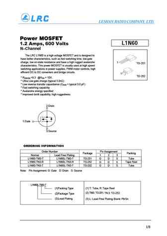
LESHAN RADIO COMPANY, LTD. Power MOSFET L1N60 1.2 Amps, 600 Volts N Channel The LRC L1N60 is a high voltage MOSFET and is designed to have better characteristics, such as fast switching time, low gate charge, low on-state resistance and have a high rugged avalanche 1 TO- 251 characteristics. This power MOSFET is usually used at high speed switching applications in power suppli
l1n60a l1n60f l1n60i.pdf
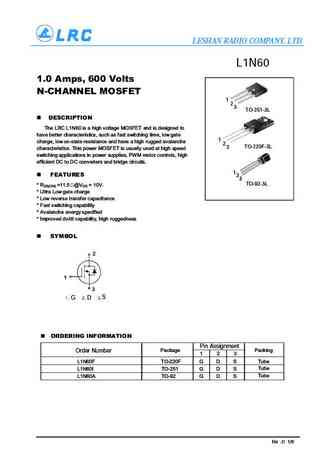
LESHAN RADIO COMPANY, LTD. L1N60 1.0 Amps, 600 Volts N-CHANNEL MOSFET 1 2 3 TO-251-3L DESCRIPTION The LRC L1N60 is a high voltage MOSFET and is designed to have better characteristics, such as fast switching time, low gate 1 charge, low on-state resistance and have a high rugged avalanche 2 3 TO-220F-3L characteristics. This power MOSFET is usually used at high speed sw
1n60af 1n60e 1n60f 1n60g.pdf
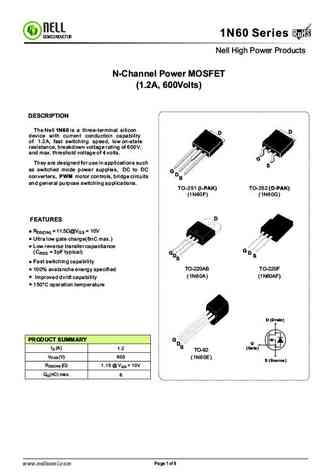
RoHS 1N60 Series RoHS SEMICONDUCTOR Nell High Power Products N-Channel Power MOSFET (1.2A, 600Volts) DESCRIPTION The Nell 1N60 is a three-terminal silicon D D device with current conduction capability of 1.2A, fast switching speed, low on-state resistance, breakdown voltage rating of 600V, and max. threshold voltage of 4 volts. G They are designed for use in applications suc
hff11n60s.pdf
HFF11N60S Shantou Huashan Electronic Devices Co., Ltd. N-Channel Enhancement Mode Field Effect Transistor General Description These are N-Channel enhancement mode silicon gate power field effect transistors. TO-220F They are advanced power MOSFETs designed, this advanced technology has been especially tailored to minimize on-state resistance, provide superior switching performa
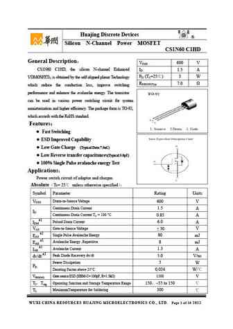
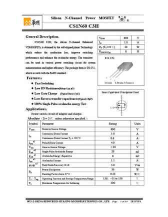
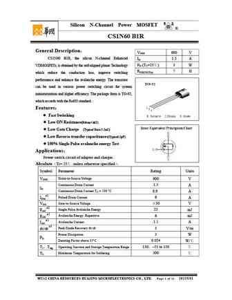
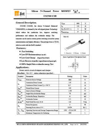
cs1n60 c1h.pdf

Silicon N-Channel Power MOSFET R CS1N60 C1H General Description VDSS 600 V CS1N60 C1H-BD, the silicon N-channel Enhanced ID 1.0 A PD (TC=25 ) 3 W VDMOSFETs, is obtained by the self-aligned planar Technology RDS(ON)Typ 9 which reduce the conduction loss, improve switching performance and enhance the avalanche energy. The transistor can be used in various power
cs1n60 a1h.pdf
Silicon N-Channel Power MOSFET R CS1N60 A1H General Description VDSS 600 V CS1N60 A1H, the silicon N-channel Enhanced ID 0.8 A PD (TC=25 ) 3 W VDMOSFETs, is obtained by the self-aligned planar Technology RDS(ON)Typ 11 which reduce the conduction loss, improve switching performance and enhance the avalanche energy. The transistor can be used in various power
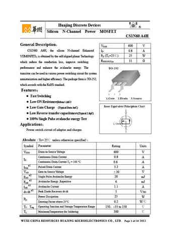
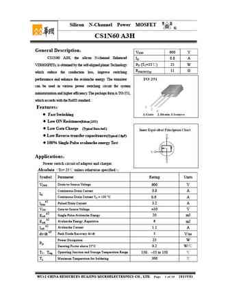
cs1n60 a3h.pdf
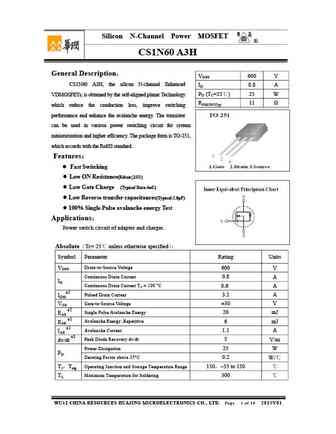
Silicon N-Channel Power MOSFET R CS1N60 A3H General Description VDSS 600 V CS1N60 A3H, the silicon N-channel Enhanced ID 0.8 A PD (TC=25 ) 25 W VDMOSFETs, is obtained by the self-aligned planar Technology RDS(ON)Typ 11 which reduce the conduction loss, improve switching performance and enhance the avalanche energy. The transistor can be used in various power
cs1n60 b1r.pdf

Silicon N-Channel Power MOSFET R CS1N60 B1R General Description VDSS 600 V CS1N60 B1R, the silicon N-channel Enhanced ID 1.5 A PD (TC=25 ) 3 W VDMOSFETs, is obtained by the self-aligned planar Technology RDS(ON)Typ 7 which reduce the conduction loss, improve switching performance and enhance the avalanche energy. The transistor can be used in various power s
cs1n60 b3r.pdf
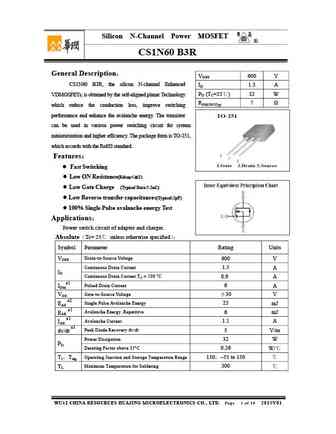
Silicon N-Channel Power MOSFET R CS1N60 B3R General Description VDSS 600 V CS1N60 B3R, the silicon N-channel Enhanced ID 1.5 A PD (TC=25 ) 32 W VDMOSFETs, is obtained by the self-aligned planar Technology RDS(ON)Typ 7 which reduce the conduction loss, improve switching performance and enhance the avalanche energy. The transistor can be used in various power s
cs1n60 c3h.pdf

Silicon N-Channel Power MOSFET R CS1N60 C3H General Description VDSS 600 V CS1N60 C3H, the silicon N-channel Enhanced ID 1.0 A PD (TC=25 ) 30 W VDMOSFETs, is obtained by the self-aligned planar Technology RDS(ON)Typ 8 which reduce the conduction loss, improve switching performance and enhance the avalanche energy. The transistor can be used in various power s
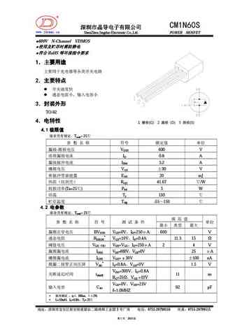
cm1n60s.pdf
R CM1N60S www.jdsemi.cn ShenZhen Jingdao Electronic Co.,Ltd. POWER MOSFET 600V N-Channel VDMOS RoHS
cm1n60c.pdf
R C16C MN0 www.jdsemi.cn ShenZhen Jingdao Electronic Co.,Ltd. POWER MOSFET 600V N-Channel VDMOS RoHS 1 2 3 TO-251 4
ftk1n60t-l.pdf
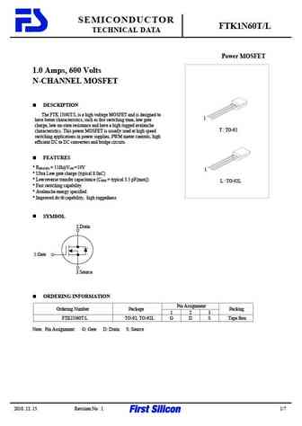
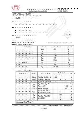
SEMICONDUCTOR FTK1N60T/L TECHNICAL DATA Power MOSFET 1.0 Amps, 600 Volts N-CHANNEL MOSFET DESCRIPTION The FTK 1N60T/L is a high voltage MOSFET and is designed to 1 have better characteristics, such as fast switching time, low gate charge, low on-state resistance and have a high rugged avalanche T TO-92 characteristics. This power MOSFET is usually used at high speed switching app
ftk1n60p f d i.pdf
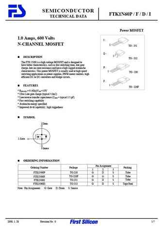
SEMICONDUCTOR FTK1N60P / F / D / I TECHNICAL DATA Power MOSFET 1.0 Amps, 600 Volts I N-CHANNEL MOSFET 1 TO - 251 D 1 DESCRIPTION TO - 252 The FTK 1N60 is a high voltage MOSFET and is designed to have better characteristics, such as fast switching time, low gate P charge, low on-state resistance and have a high rugged avalanche characteristics. This power MOSFET is usu
kx1n60ds.pdf
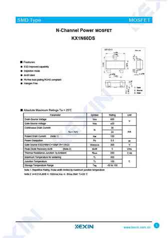
SMD Type MOSFET N-Channel Power MOSFET KX1N60DS SOT-23-3 Unit mm +0.2 2.9 -0.1 +0.1 0.4 -0.1 3 Features ESD improved capability 1 2 Depletion mode +0.02 +0.1 0.15 -0.02 0.95 -0.1 dv/dt rated +0.1 1.9 -0.2 Pb-free lead plating;ROHS compliant Halogen Free 1. Gate 2. Source 3. Drain Absolute Maximum Ratings Ta = 25 Parameter Symbol Ra
ki1n60.pdf
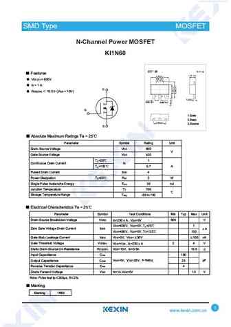
SMD Type MOSFET Transistors N-Channel Power MOSFET KI1N60 Features 1.70 0.1 VDS (V) = 600V ID = 1 A RDS(ON) 10.5 (VGS = 10V) 0.42 0.1 0.46 0.1 1.Gate 2.Drain 3.Source Absolute Maximum Ratings Ta = 25 Parameter Symbol Rating Unit Drain-Source Voltage VDS 600 V Gate-Source Voltage VGS 30 TC=25 1 Continuous Drain Current ID A TC=100 0.7 Pulsed Drain Current
ki1n60ds.pdf
SMD Type MOSFET N-Channel MOSFET KI1N60DS SOT-23-3 Unit mm +0.2 2.9-0.1 +0.1 0.4 -0.1 Features 3 VDS (V) = 600V ID = 0.4 A (VGS = 10V) RDS(ON) 30 (VGS = 10V) D 1 2 +0.02 +0.1 0.15 -0.02 0.95 -0.1 +0.1 1.9-0.2 G 1. Gate 2. Source 3. Drain S Absolute Maximum Ratings Ta = 25 Parameter Symbol Rating Unit Drain-Source Voltage VDS 600
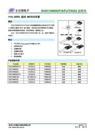
svsp11n60fjd2 svsp11n60dd2tr.pdf
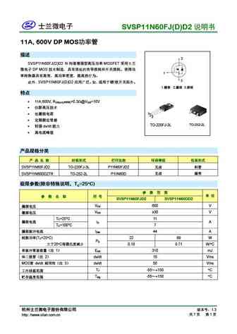
SVSP11N60FJ(D)D2 11A, 600V DP MOS 2 SVSP11N60FJ(D)D2 N MOSFET DP MOS 1 3 SVSP11N60FJ(D)D2 /
svs11n60dd2tr svs11n60fd2 svs11n60sd2 svs11n60sd2tr svs11n60fjd2 svs11n60td2 svs11n60kd2.pdf
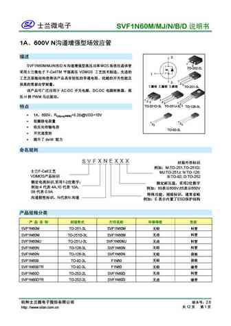
svf1n60am svf1n60amj svf1n60ab svf1n60ad svf1n60af svf1n60ah.pdf
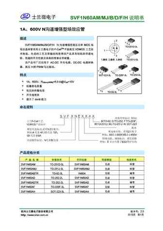
SVF1N60AM/MJ/B/D/F/H 1A 600V N 2 1 2 3 SVF1N60AM/MJ/B/D/F/H N MOS TO-251D-3L F-CellTM VDMOS 1 1 3 2 3
svsp11n60dd2tr svsp11n60fd2 svsp11n60sd2 svsp11n60sd2tr svsp11n60fjdd2 svsp11n60td2 svsp11n60kd2.pdf
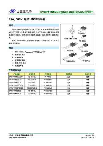
SVSP11N60D(F)(S)(FJD)(T)(K)D2 11A, 600V MOS 2 SVSP11N60D(F)(S)(FJD)(T)(K)D2 N 1 3 1 MOSFET MOS TO-263-2L 3 1 3 1. 2. 3.
mdp11n60th.pdf
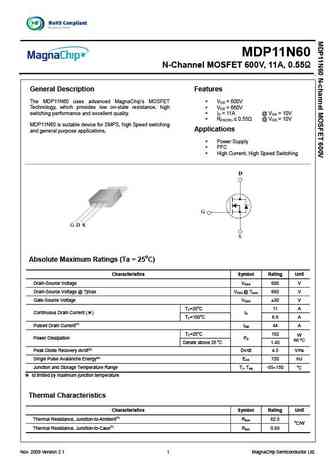
MDP11N60 N-Channel MOSFET 600V, 11A, 0.55 General Description Features The MDP11N60 uses advanced MagnaChip s MOSFET V = 600V DS Technology, which provides low on-state resistance, high V = 660V DS switching performance and excellent quality. I = 11A @ V = 10V D GS RDS(ON) 0.55 @ VGS = 10V MDP11N60 is suitable device for SMPS, high Speed switching Applications
mdz1n60umh.pdf
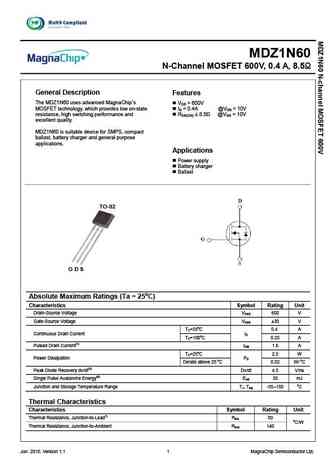
MDZ1N60 N-Channel MOSFET 600V, 0.4 A, 8.5 General Description Features The MDZ1N60 uses advanced MagnaChip s V = 600V DS MOSFET technology, which provides low on-state I = 0.4A @V = 10V D GS resistance, high switching performance and RDS(ON) 8.5 @VGS = 10V excellent quality. MDZ1N60 is suitable device for SMPS, compact ballast, battery charger and g
mdf11n60th.pdf
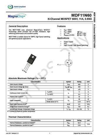
MDF11N60 N-Channel MOSFET 600V, 11A, 0.55 General Description Features The MDF11N60 uses advanced MagnaChip s MOSFET V = 600V DS Technology, which provides low on-state resistance, high V = 660V @ T DS jmax switching performance and excellent quality. I = 11A @ V = 10V D GS R 0.55 @ V = 10V DS(ON) GS MDF11N60 is suitable device for SMPS, high Spee
mdi1n60sth.pdf
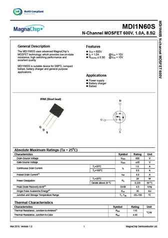
MDI1N60S N-Channel MOSFET 600V, 1.0A, 8.5 General Description Features The MDI1N60S uses advanced MagnaChip s V = 600V DS MOSFET technology, which provides low on-state ID = 1.0A @VGS = 10V resistance, high switching performance and R 8.5 @V = 10V DS(ON) GS excellent quality. MDI1N60S is suitable device for SMPS, compact ballast, battery charger and general
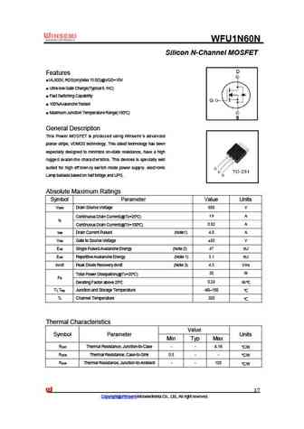
wfd1n60.pdf
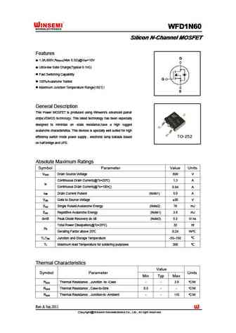
WFD1N60 WFD1N60 WFD1N60 WFD1N60 Silicon N-Channel MOSFET Silicon N-Channel MOSFET Silicon N-Channel MOSFET Silicon N-Channel MOSFET Features 1.3A,600V,R (Max 8.5 )@V =10V DS(on) GS Ultra-low Gate Charge(Typical 9.1nC) Fast Switching Capability 100%Avalanche Tested Maximum Junction Temperature Range(150 ) General Description This Power MOSFET is produced u
wfu1n60.pdf
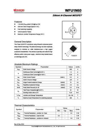
WFU1N60 WFU1N60 WFU1N60 WFU1N60 Silicon N-Channel MOSFET Silicon N-Channel MOSFET Silicon N-Channel MOSFET Silicon N-Channel MOSFET Features 1.3A,600V,R (Max 8.5 )@V =10V DS(on) GS Ultra-low Gate Charge(Typical 9.1nC) Fast Switching Capability 100%Avalanche Tested Maximum Junction Temperature Range(150 ) General Description This Power MOSFET is produced u
wfn1n60.pdf
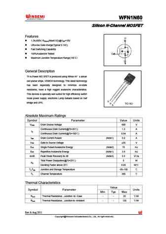
WFN1N60 WFN1N60 WFN1N60 WFN1N60 Silicon N-Channel MOSFET Silicon N-Channel MOSFET Silicon N-Channel MOSFET Silicon N-Channel MOSFET Features 1.3A,600V, R (Max8.5 )@V =10V DS(on) GS Ultra-low Gate charge(Typical 9.1nC) Fast Switching Capability 100%Avalanche Tested Maximum Junction Temperature Range(150 ) General Description Th is Power MO SFET is produced
wfn1n60n.pdf
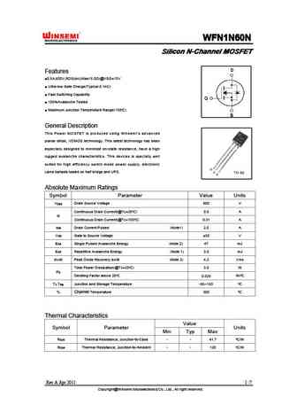
WFN1N60N WFN1N60N WFN1N60N WFN1N60N Silicon N-Channel MOSFET Silicon N-Channel MOSFET Silicon N-Channel MOSFET Silicon N-Channel MOSFET Features 0.5A,600V,RDS(on)(Max15.0 )@VGS=10V Ultra-low Gate Charge(Typical 6.1nC) Fast Switching Capability 100%Avalanche Tested Maximum Junction Temperature Range(150 ) General Description This Power MOSFET is produced usin
wfu1n60n.pdf
WFU1N60N Silicon N-Channel MOSFET Features 1A,600V, RDS(on)(Max 15.0 )@VGS=10V Ultra-low Gate Charge(Typical 6.1nC) Fast Switching Capability 100%Avalanche Tested Maximum Junction Temperature Range(150 ) General Description Th is Pow er MO S FET is pro du c ed usi ng Win se m i s ad va n ced planar stripe, VDMOS technology. This latest technology has
blv1n60a.pdf
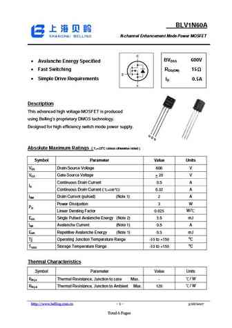
BLV1N60A N-channel Enhancement Mode Power MOSFET 600V DSS Avalanche Energy Specified BV Fast Switching RDS(ON) 15 Simple Drive Requirements ID 0.5A Description This advanced high voltage MOSFET is produced using Belling s proprietary DMOS technology. Designed for high efficiency switch mode power supply. Absolute Maximum Ratings ( TC=25oC unle
blv1n60.pdf
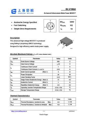
BLV1N60 N-channel Enhancement Mode Power MOSFET 600V DSS Avalanche Energy Specified BV Fast Switching RDS(ON) 8 Simple Drive Requirements ID 1A Description This advanced high voltage MOSFET is produced using Belling s proprietary DMOS technology. Designed for high efficiency switch mode power supply. Absolute Maximum Ratings ( TC=25oC unless o
cmt01n60.pdf
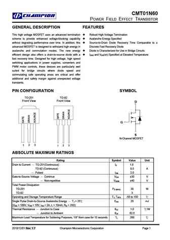
CMT01N60 POWER FIELD EFFECT TRANSISTOR GENERAL DESCRIPTION FEATURES This high voltage MOSFET uses an advanced termination Robust High Voltage Termination scheme to provide enhanced voltage-blocking capability Avalanche Energy Specified without degrading performance over time. In addition, this Source-to-Drain Diode Recovery Time Comparable to a advanced MOSFET is designed to w
ctm01n60.pdf
CTM01N60 CTM01N60 Crownpo Technology Crownpo Technology Power MOSFET Features General Description Robust High Voltage Termination This high voltage MOSFET uses an advanced termination Avalanche Energy Specified scheme to provide enhanced voltage-blocking capability Source-to-Drain Diode Recovery Time Comparable to a without degrading performance over time. In addition,
cs1n60f.pdf
BRF1N60(CS1N60F) N-CHANNEL MOSFET/N MOS DC/DC Purpose These devices are well suited for high efficiency switching DC/DC converters and switch mode power supplies. , , Features Low gate charge, low crss, fast switching. /Absolute maximum ratings(Ta=25
hy1n60d.pdf
HY1N60D / HY1N60M 600V / 1.0A 600V, RDS(ON)=12 @VGS=10V, ID=0.5A N-Channel Enhancement Mode MOSFET Features Low ON Resistance Fast Switching Low Gate Charge & Low CRSS Fully Characterized Avalanche Voltage and Current Specially Desigened for AC Adapter, Battery Charger 2 1 1 D G 2 In compliance with EU RoHs 2002/95/EC Directives G 3 DS3 S Mechanical In
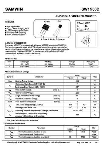
sw1n60a.pdf
SAMWIN SW1N60A N-channel MOSFET BVDSS 600V Features TO-92 ID 0.8A High ruggedness RDS(ON) 15ohm RDS(ON) (Max 15 )@VGS=10V Gate Charge (Typical 6nC) Improved dv/dt Capability 1 2 100% Avalanche Tested 2 3 1. Gate 2. Drain 3. Source 1 General Description 3 This power MOSFET is produced with advanced VDMOS technology of SAMWIN. This technology enab
swi1n60 swc1n60.pdf
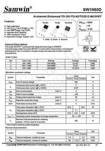
SW1N60D N-channel Enhanced TO-251/TO-92/TO251S MOSFET Features BVDSS 600V TO-251 TO-92 TO-251S ID 1A High ruggedness Low RDS(ON) (Typ 6.6 )@VGS=10V RDS(ON) 6.6 Low Gate Charge (Typ 6.8nC) Improved dv/dt Capability 2 1 1 1 100% Avalanche Tested 2 2 2 3 3 3 Application Charger, Adaptor, LED 1. Gate 2. Drain 3. Source 1
sw1n60e.pdf
SAMWIN SW1N60E Electrical characteristic ( TC = 25oC unless otherwise specified ) Symbol Parameter Test conditions Min. Typ. Max. Unit Off characteristics BVDSS Drain to source breakdown voltage VGS=0V, ID=250uA 600 V BVDSS Breakdown voltage temperature ID=250uA, referenced to 25oC 0.76 V/oC / TJ coefficient VDS=600V, VGS=0V 1 uA IDSS Drain to source leakage current
swd1n60dc swsa1n60dc.pdf
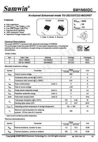
SW1N60DC N-channel Enhanced mode TO-252/SOT223 MOSFET Features TO-252 SOT223 BVDSS 600V ID 1A High ruggedness Low RDS(ON) (Typ 7 )@VGS=10V RDS(ON) 7 Low Gate Charge (Typ6.3 nC) Improved dv/dt Capability 2 100% Avalanche Tested 1 1 2 2 Application Charger,Adaptor,LED 3 3 1 1. Gate 2. Drain 3. Source 3 General Description This power MOSFET
sw1n60c.pdf
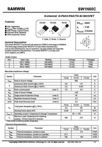
SAMWIN SW1N60C N-channel D-PAK/I-PAK/TO-92 MOSFET Features TO-251 TO-252 TO-92 BVDSS 600V High ruggedness ID 1.0A RDS(ON) (Max 9 )@VGS=10V Gate Charge (Typical 5.6nC) RDS(ON) 9.0ohm 1 2 1 Improved dv/dt Capability 2 3 1 3 2 100% Avalanche Tested 3 2 1. Gate 2. Drain 3. Source General Description 1 This power MOSFET is produced with advanced V
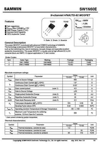
sw1n60d.pdf
SAMWIN SW1N60D N-channel I-PAK/TO-92 MOSFET TO-92 TO-251 Features BVDSS 600V ID 1A High ruggedness RDS(ON) (Max8.5 )@VGS=10V RDS(ON) 8.5 Gate Charge (Typical 6.8 nC) Improved dv/dt Capability 1 100% Avalanche Tested 1 2 2 2 3 3 1. Gate 2. Drain 3. Source 1 General Description This power MOSFET is produced with advanced VDMOS
hfu1n60f hfd1n60f.pdf
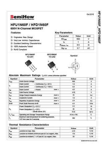
Oct 2016 HFU1N60F / HFD1N60F 600V N-Channel MOSFET Features Key Parameters Parameter Value Unit Originative New Design BVDSS 600 V Very Low Intrinsic Capacitances ID 1A Excellent Switching Characteristics RDS(on), Typ 6.5 100% Avalanche Tested Qg, Typ 3.7 nC RoHS Compliant HFU1N60F HFD1N60F Symbol TO-251 TO-252 D S S D G G Absolute Maximum Ratings TC=25 unless
hft1n60s.pdf
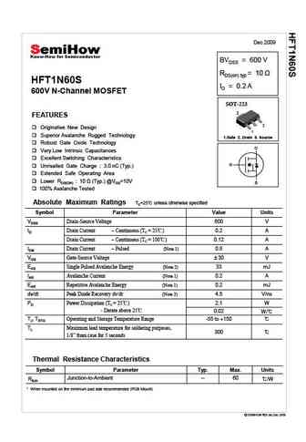
Dec 2009 BVDSS = 600 V RDS(on) typ HFT1N60S ID = 0.2 A 600V N-Channel MOSFET SOT-223 2 FEATURES 3 Originative New Design 1 Superior Avalanche Rugged Technology 1.Gate 2. Drain 3. Source Robust Gate Oxide Technology D Very Low Intrinsic Capacitances Excellent Switching Characteristics G Unrivalled Gate Charge 3.0 nC (Typ.) Extended Safe Operating Area Lowe
hft1n60f.pdf
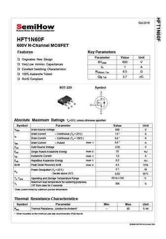
Oct 2016 HFT1N60F 600V N-Channel MOSFET Features Key Parameters Parameter Value Unit Originative New Design BVDSS 600 V Very Low Intrinsic Capacitances ID 1A Excellent Switching Characteristics RDS(on), Typ 6.5 100% Avalanche Tested Qg, Typ 3.7 nC RoHS Compliant SOT-223 Symbol S D G Absolute Maximum Ratings TC=25 unless otherwise specified Symbol Parameter Value U
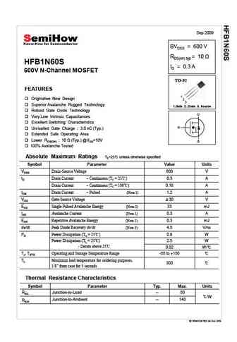
hfb1n60s.pdf
Sep 2009 BVDSS = 600 V RDS(on) typ HFB1N60S ID = 0.3 A 600V N-Channel MOSFET TO-92 FEATURES 1 Originative New Design 2 3 Superior Avalanche Rugged Technology 1.Gate 2. Drain 3. Source Robust Gate Oxide Technology D Very Low Intrinsic Capacitances Excellent Switching Characteristics G Unrivalled Gate Charge 3.0 nC (Typ.) Extended Safe Operating Area
hfd1n60s hfu1n60s.pdf
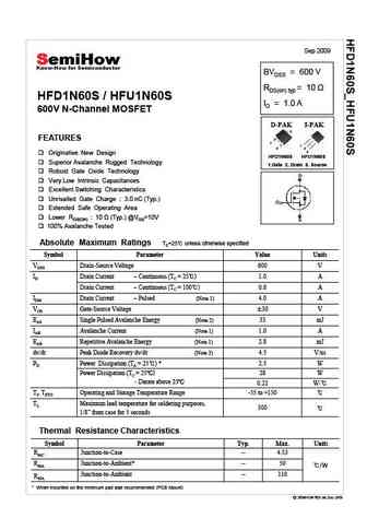
Sep 2009 BVDSS = 600 V RDS(on) typ HFD1N60S / HFU1N60S ID = 1.0 A 600V N-Channel MOSFET D-PAK I-PAK 2 FEATURES 1 1 3 2 3 Originative New Design HFD1N60S HFU1N60S Superior Avalanche Rugged Technology 1.Gate 2. Drain 3. Source Robust Gate Oxide Technology Very Low Intrinsic Capacitances Excellent Switching Characteristics Unrivalled Gate Charge 3.0 nC (T
hfd1n60s.pdf

Sep 2009 BVDSS = 600 V RDS(on) typ HFD1N60S / HFU1N60S ID = 1.0 A 600V N-Channel MOSFET D-PAK I-PAK 2 FEATURES 1 1 3 2 3 Originative New Design HFD1N60S HFU1N60S Superior Avalanche Rugged Technology 1.Gate 2. Drain 3. Source Robust Gate Oxide Technology Very Low Intrinsic Capacitances Excellent Switching Characteristics Unrivalled Gate Charge 3.0 nC (T
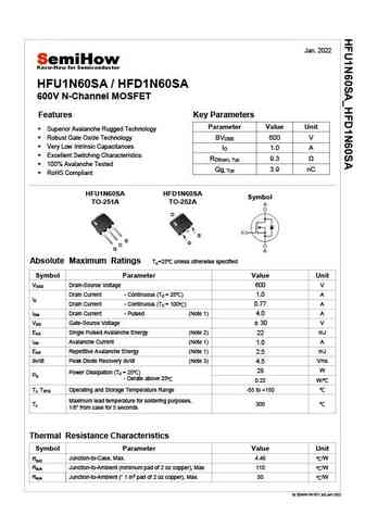
hfu1n60sa hfd1n60sa.pdf
Jan. 2022 HFU1N60SA / HFD1N60SA 600V N-Channel MOSFET Features Key Parameters Parameter Value Unit Superior Avalanche Rugged Technology BVDSS 600 V Robust Gate Oxide Technology Very Low Intrinsic Capacitances ID 1.0 A Excellent Switching Characteristics RDS(on), Typ 9.3 100% Avalanche Tested Qg, Typ 3.9 nC RoHS Compliant HFU1N60SA HFD1N60SA Symbol TO-
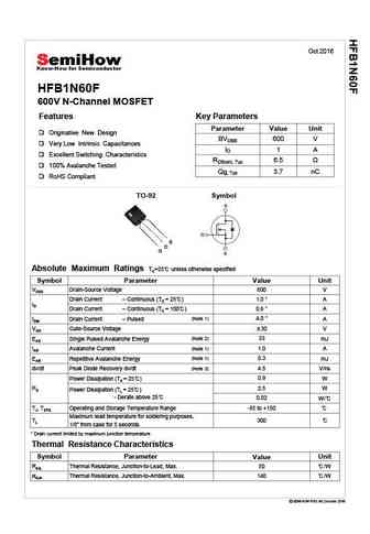
hfb1n60f.pdf
Oct 2016 HFB1N60F 600V N-Channel MOSFET Features Key Parameters Parameter Value Unit Originative New Design BVDSS 600 V Very Low Intrinsic Capacitances ID 1A Excellent Switching Characteristics RDS(on), Typ 6.5 100% Avalanche Tested Qg, Typ 3.7 nC RoHS Compliant TO-92 Symbol S D G Absolute Maximum Ratings TC=25 unless otherwise specified Symbol Parameter Value Uni
msu1n60.pdf
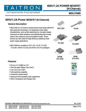
600V/1.2A POWER MOSFET (N-Channel) MSU1N60 600V/1.2A Power MOSFET (N-Channel) General Description MSU1N60 is a N-Channel enhancement mode power MOSFET SOT-223 TO-92 with advanced technology. It is designed to have better characteristics, such as fast switching time, low gate charge, minimized on-state resistance and withstanding high energy pulse in the avalanche an
cs1n60c1hd.pdf
Huajing Discrete Devices R Silicon N-Channel Power MOSFET CS1N60 C1HD General Description VDSS 600 V CS1N60 C1HD, the silicon N-channel Enhanced ID 1.5 A PD (TC=25 ) 3 W VDMOSFETs, is obtained by the self-aligned planar Technology RDS(ON)Typ 7.0 which reduce the conduction loss, improve switching performance and enhance the avalanche energy. The transistor
cs1n60a1h.pdf

Silicon N-Channel Power MOSFET R CS1N60 A1H General Description VDSS 600 V CS1N60 A1H, the silicon N-channel Enhanced ID 0.8 A PD (TC=25 ) 3 W VDMOSFETs, is obtained by the self-aligned planar Technology RDS(ON)Typ 11 which reduce the conduction loss, improve switching performance and enhance the avalanche energy. The transistor can be used in various power
cs1n60c3h.pdf
Silicon N-Channel Power MOSFET R CS1N60 C3H General Description VDSS 600 V CS1N60 C3H, the silicon N-channel Enhanced ID 1.0 A PD (TC=25 ) 30 W VDMOSFETs, is obtained by the self-aligned planar Technology RDS(ON)Typ 8 which reduce the conduction loss, improve switching performance and enhance the avalanche energy. The transistor can be used in various power s
cs1n60b1r.pdf
Silicon N-Channel Power MOSFET R CS1N60 B1R General Description VDSS 600 V CS1N60 B1R, the silicon N-channel Enhanced ID 1.5 A PD (TC=25 ) 3 W VDMOSFETs, is obtained by the self-aligned planar Technology RDS(ON)Typ 7 which reduce the conduction loss, improve switching performance and enhance the avalanche energy. The transistor can be used in various power s
cs1n60c1h.pdf
Silicon N-Channel Power MOSFET R CS1N60 C1H General Description VDSS 600 V CS1N60 C1H-BD, the silicon N-channel Enhanced ID 1.0 A PD (TC=25 ) 3 W VDMOSFETs, is obtained by the self-aligned planar Technology RDS(ON)Typ 9 which reduce the conduction loss, improve switching performance and enhance the avalanche energy. The transistor can be used in various power
cs1n60a4h.pdf
Huajing Discrete Devices R Silicon N-Channel Power MOSFET CS1N60 A4H General Description VDSS 600 V CS1N60 A4H, the silicon N-channel Enhanced ID 0.8 A PD (TC=25 ) 25 W VDMOSFETs, is obtained by the self-aligned planar Technology RDS(ON)Typ 11 which reduce the conduction loss, improve switching performance and enhance the avalanche energy. The transistor
cs1n60b3r.pdf

Silicon N-Channel Power MOSFET R CS1N60 B3R General Description VDSS 600 V CS1N60 B3R, the silicon N-channel Enhanced ID 1.5 A PD (TC=25 ) 32 W VDMOSFETs, is obtained by the self-aligned planar Technology RDS(ON)Typ 7 which reduce the conduction loss, improve switching performance and enhance the avalanche energy. The transistor can be used in various power s
cs1n60a3h.pdf
Silicon N-Channel Power MOSFET R CS1N60 A3H General Description VDSS 600 V CS1N60 A3H, the silicon N-channel Enhanced ID 0.8 A PD (TC=25 ) 25 W VDMOSFETs, is obtained by the self-aligned planar Technology RDS(ON)Typ 11 which reduce the conduction loss, improve switching performance and enhance the avalanche energy. The transistor can be used in various power
1n60l-tm3-t.pdf
1N60L-TM3-T www.VBsemi.tw N hannel 650 D S Power MOSFET FEATURES PRODUCT SUMMARY Low Gate Charge Qg Results in Simple Drive VDS (V) 650 Available Requirement RDS(on) ( )VGS = 10 V 5 RoHS Improved Gate, Avalanche and Dynamic dV/dt COMPLIANT Qg (Max.) (nC) 11 Ruggedness Qgs (nC) 2.3 Fully Characterized Capacitance and Avalanche Voltage and Current Qgd (nC) 5.
hms11n60d hms11n60 hms11n60f.pdf
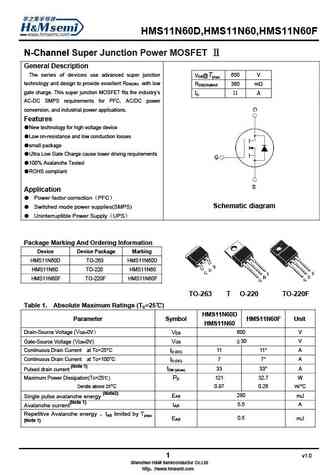
HMS11N60D,HMS11N60,HMS11N60F N-Channel Super Junction Power MOSFET General Description The series of devices use advanced super junction 650 V VDS@Tjmax technology and design to provide excellent RDS(ON) with low RDS(ON)MAX 360 m gate charge. This super junction MOSFET fits the industry s ID 11 A AC-DC SMPS requirements for PFC, AC/DC power conversion, and industrial p
hms11n60k hms11n60i.pdf
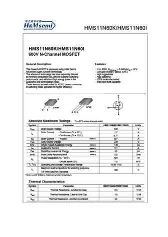
HMS11N60K/HMS11N60I HMS11N60K/HMS11N60I 600V N-Channel MOSFET General Description Features This Power MOSFET is produced using H&M Semi s - 11A, 600V, RDS(on) typ. = 0.34 @VGS = 10 V Advanced Super-Junction technology. - Low gate charge ( typical 33nC) This advanced technology has been especially tailored - High ruggedness to minimize conduction loss, provide superior switching - Fast
hms21n60a.pdf
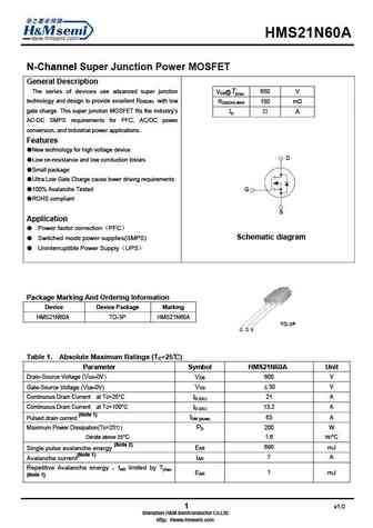
HMS21N60A N-Channel Super Junction Power MOSFET General Description The series of devices use advanced super junction 650 V VDS@Tjmax technology and design to provide excellent RDS(ON) with low RDS(ON) MAX 180 m gate charge. This super junction MOSFET fits the industry s ID 21 A AC-DC SMPS requirements for PFC, AC/DC power conversion, and industrial power applications. F
hm1n60r.pdf
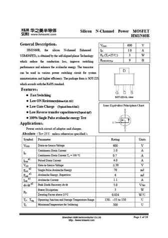
Silicon N-Channel Power MOSFET HM1N60R General Description VDSS 600 V HM1N60R, the silicon N-channel Enhanced ID 1.0 A PD (TC=25 ) 3 W VDMOSFETs, is obtained by the self-aligned planar Technology RDS(ON)Typ 9 which reduce the conduction loss, improve switching performance and enhance the avalanche energy. The transistor can be used in various power switching circuit fo
hms21n60 hms21n60f.pdf
HMS21N60,HMS21N60F N-Channel Super Junction Power MOSFET II General Description The series of devices use advanced super junction 650 V VDS@Tjmax technology and design to provide excellent RDS(ON) with low RDS(ON) MAX 180 m gate charge. This super junction MOSFET fits the industry s ID 21 A AC-DC SMPS requirements for PFC, AC/DC power conversion, and industrial power applica
hm1n60.pdf
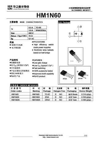
N N-CHANNEL MOSFET MAIN CHARACTERISTICS Package 0.5 A TO-92 ID 1.0 A IPAK/DPKA VDSS 600 V Rdson Vgs=10V 15 Qg 6.1 nC APPLICATIONS High efficiency switch mode power supplies Electronic lamp ballasts based on half bridge FEATU
hm1n60pr.pdf
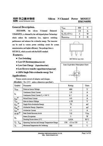
Silicon N-Channel Power MOSFET HM1N60 General Description VDSS 600 V HM1N60PR, the silicon N-channel Enhanced ID 1.0 A PD (TC=25 ) 3 W VDMOSFETs, is obtained by the self-aligned planar Technology RDS(ON)Typ 9 which reduce the conduction loss, improve switching performance and enhance the avalanche energy. The transistor can be used in various power switching circu
h1n60u h1n60d.pdf
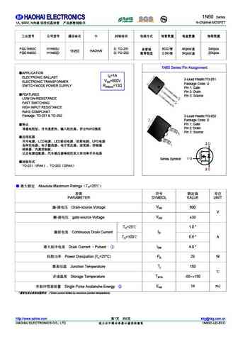
1N60 Series N-Channel MOSFET 1A, 600V, N H FQU1N60C H1N60U U TO-251 80 / 4Kpcs/ 24Kpcs HAOHAI 1N60 FQD1N60C H1N60D D TO-252 25Kpcs 2.5K/ 5Kpcs/ 1N60 Series Pin Assignment APPLICATION ID=1A
spw11n60cfd.pdf
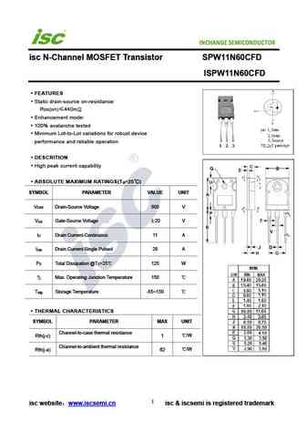
INCHANGE Semiconductor isc N-Channel MOSFET Transistor SPW11N60CFD ISPW11N60CFD FEATURES Static drain-source on-resistance RDS(on) 440m Enhancement mode 100% avalanche tested Minimum Lot-to-Lot variations for robust device performance and reliable operation DESCRITION High peak current capability ABSOLUTE MAXIMUM RATINGS(T =25 ) a SYMBOL PARAMETER VALUE UN
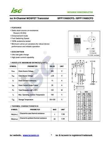
spp11n60cfd.pdf
isc N-Channel MOSFET Transistor SPP11N60CFD ISPP11N60CFD FEATURES Static drain-source on-resistance RDS(on) 0.44 Enhancement mode Fast Switching Speed 100% avalanche tested Minimum Lot-to-Lot variations for robust device performance and reliable operation DESCRIPTION Ultra low gate charge High peak current capability ABSOLUTE MAXIMUM RATINGS(T =25 )
spu01n60c3.pdf
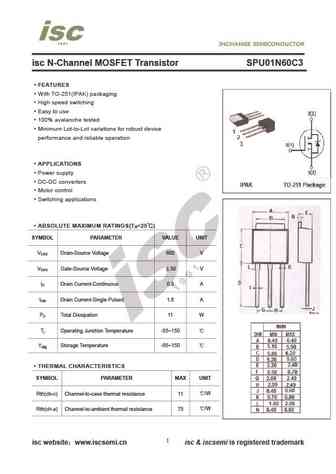
isc N-Channel MOSFET Transistor SPU01N60C3 FEATURES With TO-251(IPAK) packaging High speed switching Easy to use 100% avalanche tested Minimum Lot-to-Lot variations for robust device performance and reliable operation APPLICATIONS Power supply DC-DC converters Motor control Switching applications ABSOLUTE MAXIMUM RATINGS(T =25 ) a SYMBOL PARAMETER VALUE
fcp11n60n.pdf
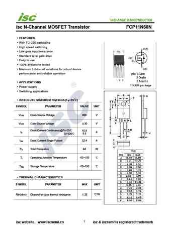
isc N-Channel MOSFET Transistor FCP11N60N FEATURES With TO-220 packaging High speed switching Low gate input resistance Standard level gate drive Easy to use 100% avalanche tested Minimum Lot-to-Lot variations for robust device performance and reliable operation APPLICATIONS Power supply Switching applications ABSOLUTE MAXIMUM RATINGS(T =25 ) a SYMBOL PA
spp11n60c3.pdf
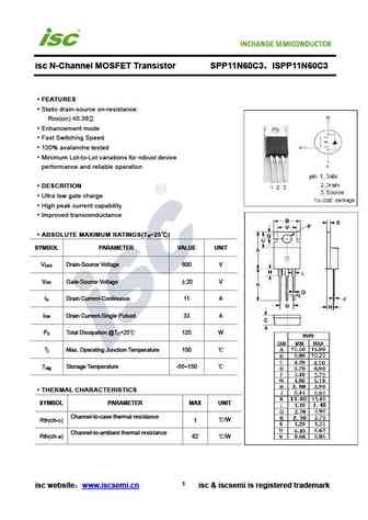
isc N-Channel MOSFET Transistor SPP11N60C3 ISPP11N60C3 FEATURES Static drain-source on-resistance RDS(on) 0.38 Enhancement mode Fast Switching Speed 100% avalanche tested Minimum Lot-to-Lot variations for robust device performance and reliable operation DESCRITION Ultra low gate charge High peak current capability Improved transconductance ABSOLUTE MA
irfr1n60a.pdf
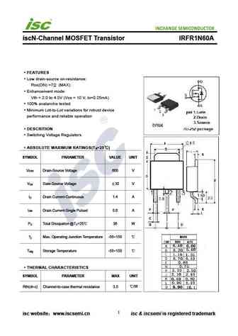
iscN-Channel MOSFET Transistor IRFR1N60A FEATURES Low drain-source on-resistance RDS(ON) =7 (MAX) Enhancement mode Vth = 2.0 to 4.0V (VDS = 10 V, ID=0.25mA) 100% avalanche tested Minimum Lot-to-Lot variations for robust device performance and reliable operation DESCRITION Switching Voltage Regulators ABSOLUTE MAXIMUM RATINGS(T =25 ) a SYMBOL PARAMETER VALUE U
fmv11n60e.pdf
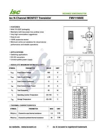
INCHANGE Semiconductor isc N-Channel MOSFET Transistor FMV11N60E FEATURES With TO-220F packaging Maintains both low power loss andlow noise Very high commutation ruggedness Easy to use 100% avalanche tested Minimum Lot-to-Lot variations for robust device performance and reliable operationz APPLICATIONS Switching applications DC-DC converters Uninterruptible po
spw11n60c3.pdf
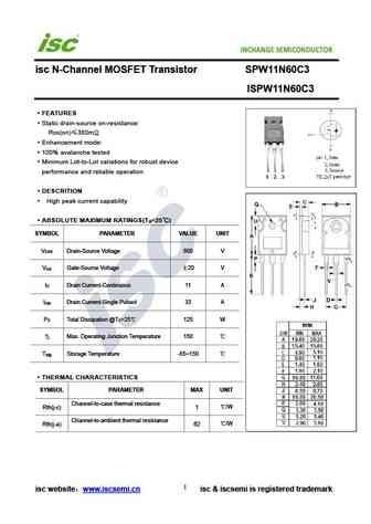
INCHANGE Semiconductor isc N-Channel MOSFET Transistor SPW11N60C3 ISPW11N60C3 FEATURES Static drain-source on-resistance RDS(on) 380m Enhancement mode 100% avalanche tested Minimum Lot-to-Lot variations for robust device performance and reliable operation DESCRITION High peak current capability ABSOLUTE MAXIMUM RATINGS(T =25 ) a SYMBOL PARAMETER VALUE UNI
spa11n60c3.pdf
INCHANGE Semiconductor isc N-Channel MOSFET Transistor SPA11N60C3 FEATURES New revolutionary high voltage technology Ultra low gate charge High peak current capability Improved transconductance 100% avalanche tested Minimum Lot-to-Lot variations for robust device performance and reliable operation APPLICATIONS Switching applications ABSOLUTE MAXIMUM RATINGS(T =25
spb11n60c3.pdf
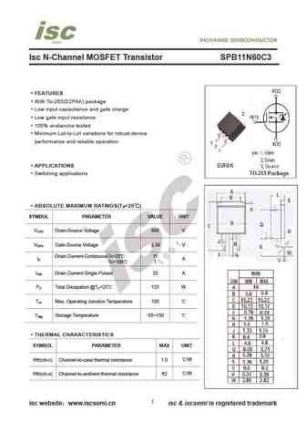
Isc N-Channel MOSFET Transistor SPB11N60C3 FEATURES With To-263(D2PAK) package Low input capacitance and gate charge Low gate input resistance 100% avalanche tested Minimum Lot-to-Lot variations for robust device performance and reliable operation APPLICATIONS Switching applications ABSOLUTE MAXIMUM RATINGS(T =25 ) a SYMBOL PARAMETER VALUE UNIT V Drain-Source Vo
irfu1n60a.pdf
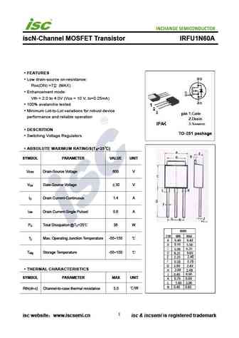
iscN-Channel MOSFET Transistor IRFU1N60A FEATURES Low drain-source on-resistance RDS(ON) =7 (MAX) Enhancement mode Vth = 2.0 to 4.0V (VDS = 10 V, ID=0.25mA) 100% avalanche tested Minimum Lot-to-Lot variations for robust device performance and reliable operation DESCRITION Switching Voltage Regulators ABSOLUTE MAXIMUM RATINGS(T =25 ) a SYMBOL PARAMETER VALUE U
mdp11n60th.pdf
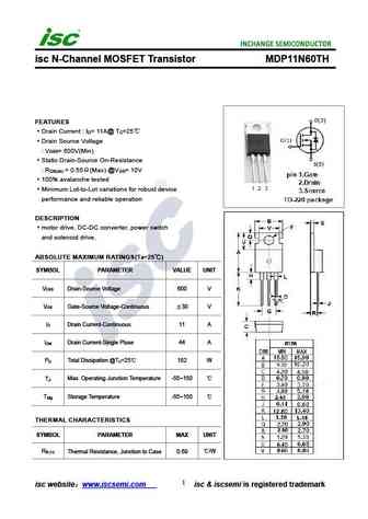
isc N-Channel MOSFET Transistor MDP11N60TH FEATURES Drain Current I = 11A@ T =25 D C Drain Source Voltage V = 600V(Min) DSS Static Drain-Source On-Resistance R = 0.55 (Max) @V = 10V DS(on) GS 100% avalanche tested Minimum Lot-to-Lot variations for robust device performance and reliable operation DESCRIPTION motor drive, DC-DC converter, power switch and sole
aob11n60.pdf
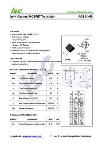
isc N-Channel MOSFET Transistor AOB11N60 FEATURES Drain Current I = 11A@ T =25 D C Drain Source Voltage- V = 600V(Min) DSS Static Drain-Source On-Resistance R = 0.7 (Max) DS(on) 100% avalanche tested Minimum Lot-to-Lot variations for robust device performance and reliable operation DESCRIPTION Designed for use in switch mode power supplies and general purpo
spa11n60c3e8185.pdf
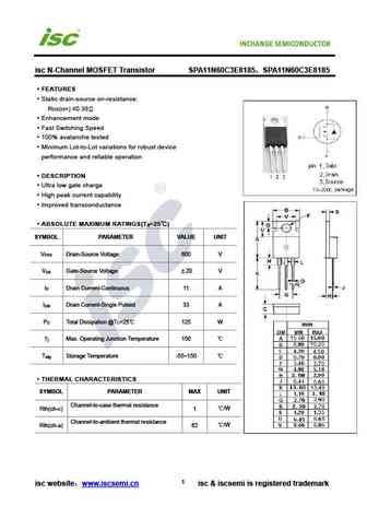
isc N-Channel MOSFET Transistor SPA11N60C3E8185 SPA11N60C3E8185 FEATURES Static drain-source on-resistance RDS(on) 0.38 Enhancement mode Fast Switching Speed 100% avalanche tested Minimum Lot-to-Lot variations for robust device performance and reliable operation DESCRIPTION Ultra low gate charge High peak current capability Improved transconductance A
aou1n60.pdf
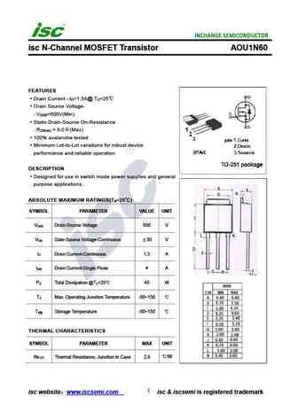
isc N-Channel MOSFET Transistor AOU1N60 FEATURES Drain Current I =1.3A@ T =25 D C Drain Source Voltage- V =600V(Min) DSS Static Drain-Source On-Resistance R = 9.0 (Max) DS(on) 100% avalanche tested Minimum Lot-to-Lot variations for robust device performance and reliable operation DESCRIPTION Designed for use in switch mode power supplies and general purpose
aotf11n60.pdf
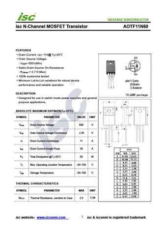
isc N-Channel MOSFET Transistor AOTF11N60 FEATURES Drain Current I = 11A@ T =25 D C Drain Source Voltage- V = 600V(Min) DSS Static Drain-Source On-Resistance R = 0.7 (Max) DS(on) 100% avalanche tested Minimum Lot-to-Lot variations for robust device performance and reliable operation DESCRIPTION Designed for use in switch mode power supplies and general purp
spw11n60s5.pdf
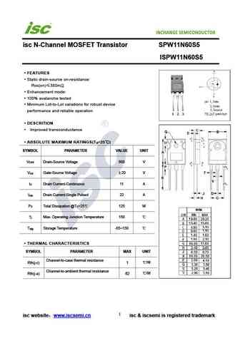
INCHANGE Semiconductor isc N-Channel MOSFET Transistor SPW11N60S5 ISPW11N60S5 FEATURES Static drain-source on-resistance RDS(on) 380m Enhancement mode 100% avalanche tested Minimum Lot-to-Lot variations for robust device performance and reliable operation DESCRITION Improved transconductance ABSOLUTE MAXIMUM RATINGS(T =25 ) a SYMBOL PARAMETER VALUE UNIT
aot1n60.pdf
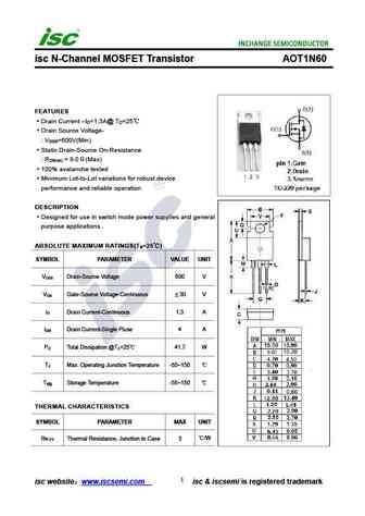
isc N-Channel MOSFET Transistor AOT1N60 FEATURES Drain Current I =1.3A@ T =25 D C Drain Source Voltage- V =600V(Min) DSS Static Drain-Source On-Resistance R = 9.0 (Max) DS(on) 100% avalanche tested Minimum Lot-to-Lot variations for robust device performance and reliable operation DESCRIPTION Designed for use in switch mode power supplies and general purpose
fch041n60f.pdf
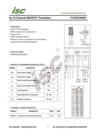
isc N-Channel MOSFET Transistor FCH041N60F FEATURES With TO-247 packaging With low gate drive requirements Easy to drive 100% avalanche tested Minimum Lot-to-Lot variations for robust device performance and reliable operation APPLICATIONS Switching applications ABSOLUTE MAXIMUM RATINGS(T =25 ) a SYMBOL PARAMETER VALUE UNIT V Drain-Source Voltage 600 V DSS V Ga
aot11n60.pdf
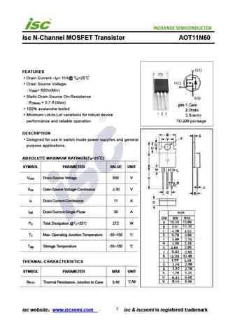
isc N-Channel MOSFET Transistor AOT11N60 FEATURES Drain Current I = 11A@ T =25 D C Drain Source Voltage- V = 600V(Min) DSS Static Drain-Source On-Resistance R = 0.7 (Max) DS(on) 100% avalanche tested Minimum Lot-to-Lot variations for robust device performance and reliable operation DESCRIPTION Designed for use in switch mode power supplies and general purpo
aoi1n60.pdf

isc N-Channel MOSFET Transistor AOI1N60 FEATURES Drain Current I =1.3A@ T =25 D C Drain Source Voltage- V =600V(Min) DSS Static Drain-Source On-Resistance R = 9.0 (Max) DS(on) 100% avalanche tested Minimum Lot-to-Lot variations for robust device performance and reliable operation DESCRIPTION Designed for use in switch mode power supplies and general purpose
irfp21n60l.pdf
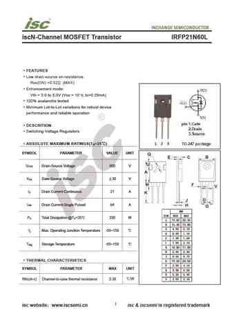
iscN-Channel MOSFET Transistor IRFP21N60L FEATURES Low drain-source on-resistance RDS(ON) =0.32 (MAX) Enhancement mode Vth = 3.0 to 5.0V (VDS = 10 V, ID=0.25mA) 100% avalanche tested Minimum Lot-to-Lot variations for robust device performance and reliable operation DESCRITION Switching Voltage Regulators ABSOLUTE MAXIMUM RATINGS(T =25 ) a SYMBOL PARAMETER VAL
spa11n60cfd.pdf
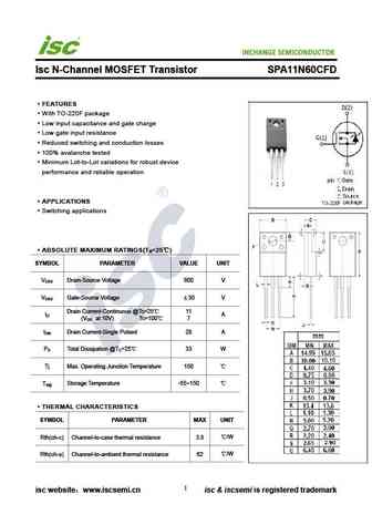
INCHANGE Semiconductor Isc N-Channel MOSFET Transistor SPA11N60CFD FEATURES With TO-220F package Low input capacitance and gate charge Low gate input resistance Reduced switching and conduction losses 100% avalanche tested Minimum Lot-to-Lot variations for robust device performance and reliable operation APPLICATIONS Switching applications ABSOLUTE MAXIMUM RATING
spb11n60s5.pdf

Isc N-Channel MOSFET Transistor SPB11N60S5 FEATURES With To-263(D2PAK) package Low input capacitance and gate charge Low gate input resistance 100% avalanche tested Minimum Lot-to-Lot variations for robust device performance and reliable operation APPLICATIONS Switching applications ABSOLUTE MAXIMUM RATINGS(T =25 ) a SYMBOL PARAMETER VALUE UNIT V Drain-Source Vo
tk31n60w.pdf
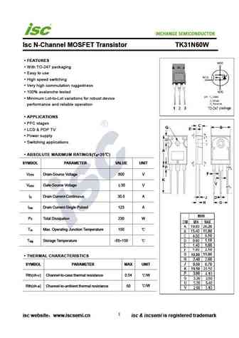
INCHANGE Semiconductor Isc N-Channel MOSFET Transistor TK31N60W FEATURES With TO-247 packaging Easy to use High speed switching Very high commutation ruggedness 100% avalanche tested Minimum Lot-to-Lot variations for robust device performance and reliable operation APPLICATIONS PFC stages LCD & PDP TV Power supply Switching applications ABSOLUTE MAXIMUM
fcpf11n60nt.pdf
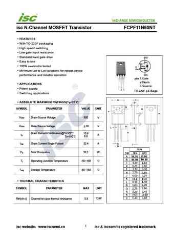
isc N-Channel MOSFET Transistor FCPF11N60NT FEATURES With TO-220F packaging High speed switching Low gate input resistance Standard level gate drive Easy to use 100% avalanche tested Minimum Lot-to-Lot variations for robust device performance and reliable operation APPLICATIONS Power supply Switching applications ABSOLUTE MAXIMUM RATINGS(T =25 ) a SYMBOL
aod1n60.pdf
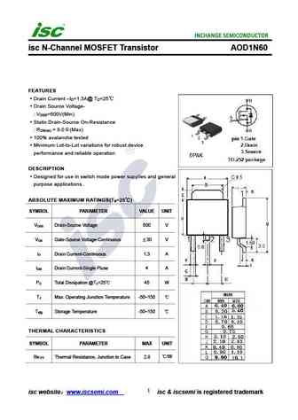
isc N-Channel MOSFET Transistor AOD1N60 FEATURES Drain Current I =1.3A@ T =25 D C Drain Source Voltage- V =600V(Min) DSS Static Drain-Source On-Resistance R = 9.0 (Max) DS(on) 100% avalanche tested Minimum Lot-to-Lot variations for robust device performance and reliable operation DESCRIPTION Designed for use in switch mode power supplies and general purpose
aow11n60.pdf
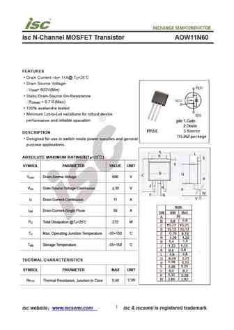
isc N-Channel MOSFET Transistor AOW11N60 FEATURES Drain Current I = 11A@ T =25 D C Drain Source Voltage- V = 600V(Min) DSS Static Drain-Source On-Resistance R = 0.7 (Max) DS(on) 100% avalanche tested Minimum Lot-to-Lot variations for robust device performance and reliable operation DESCRIPTION Designed for use in switch mode power supplies and general purpo
Otros transistores... 12N60 , 15N60 , 18N60 , 20N60 , 22N60 , UF601 , UK2996 , 1N60A , IRF740 , 1N60P , 1N60Z , 2N60L , 2N60 , 2N60K , 3N60 , 3N60A , 3N60Z .
🌐 : EN ES РУ

Liste
Recientemente añadidas las descripciónes de los transistores:
MOSFET: 2N7002KM | 2N7002KH | AON5802 | AOSS62934 | AOSN21319C | AONS66966 | AONR62992 | AON7400B | AON6578 | AO3480C | AO3400C | HAF1008S | HAF1008L | EMZB08P03H | CS30N20FA9R | AOT66613L
Popular searches
bd243 | 2sk170 datasheet | 2n7000 equivalent | tip31 | tip122 transistor | 2sc1079 | 2sc1815 equivalent | 2sa1220