AOT500 MOSFET Equivalente. Reemplazo. Hoja de especificaciones. Principales características
Número de Parte: AOT500
Tipo de FET: MOSFET
Polaridad de transistor: N
ESPECIFICACIONES MÁXIMAS
Pdⓘ - Máxima disipación de potencia: 115 W
|Vds|ⓘ - Voltaje máximo drenador-fuente: 33 V
|Vgs|ⓘ - Voltaje máximo fuente-puerta: 20 V
|Id|ⓘ - Corriente continua de drenaje: 80 A
Tjⓘ - Temperatura máxima de unión: 175 °C
CARACTERÍSTICAS ELÉCTRICAS
trⓘ - Tiempo de subida: 35 nS
Cossⓘ - Capacitancia de salida: 765 pF
RDSonⓘ - Resistencia estado encendido drenaje a fuente: 0.0053 Ohm
Encapsulados: TO-220
Búsqueda de reemplazo de AOT500 MOSFET
- Selecciónⓘ de transistores por parámetros
AOT500 datasheet
aot500.pdf
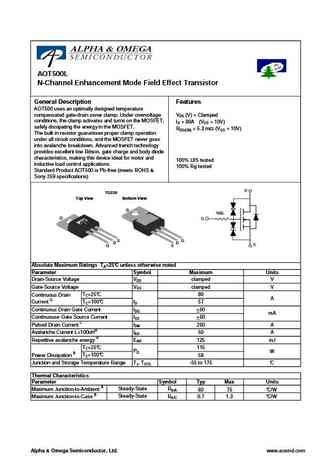
AOT500L N-Channel Enhancement Mode Field Effect Transistor General Description Features AOT500 uses an optimally designed temperature compensated gate-drain zener clamp. Under overvoltage VDS (V) = Clamped conditions, the clamp activates and turns on the MOSFET, ID = 80A (VGS = 10V) safely dissipating the energy in the MOSFET. RDS(ON)
aot502.pdf
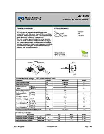
AOT502 Clamped N-Channel MOSFET General Description Product Summary VDS Clamped AOT502 uses an optimally designed temperature 60A ID (at VGS=10V) compensated gate-drain zener clamp. Under overvoltage conditions, the clamp activates and turns on the MOSFET,
aot502.pdf
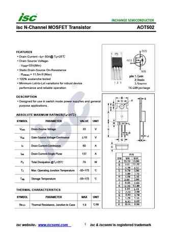
isc N-Channel MOSFET Transistor AOT502 FEATURES Drain Current I = 60A@ T =25 D C Drain Source Voltage- V =33V(Min) DSS Static Drain-Source On-Resistance R = 11.5m (Max) DS(on) 100% avalanche tested Minimum Lot-to-Lot variations for robust device performance and reliable operation DESCRIPTION Designed for use in switch mode power supplies and general purpose
Otros transistores... AOT466L, AOT470, AOT472, AOT474, AOT480L, AOT482L, AOT4N60, AOT4S60, 75N75, AOT502, AOT5N100, AOT5N50, AOT5N60, AOT7N60, AOT7N65, AOT7N70, AOT7S60
History: RFP2N08L | IRFBG30PBF
🌐 : EN ES РУ

Liste
Recientemente añadidas las descripciónes de los transistores:
MOSFET: FTF30P35D | FTF25N35DHVT | FTF15N35D | FTE15C35G | FTP02P15G | FTE02P15G | AKF30N5P0SX | AKF30N10S | AKF20P45D | CM4407 | CM3407 | CM3400 | SVF11N65F | SVF11N65T | FKBB3105 | EHBA036R1
Popular searches
2sc2240 | bc547 transistor equivalent | 2sa1943 | tip41c datasheet | mje15032 | tip32c datasheet | mje15032g | irf1404