P75N02LDG MOSFET Equivalente. Reemplazo. Hoja de especificaciones. Principales características
Número de Parte: P75N02LDG
Tipo de FET: MOSFET
Polaridad de transistor: N
ESPECIFICACIONES MÁXIMAS
Pdⓘ - Máxima
disipación de potencia: 54 W
|Vds|ⓘ - Voltaje máximo drenador-fuente: 25 V
|Vgs|ⓘ - Voltaje máximo fuente-puerta: 20 V
|Id|ⓘ - Corriente continua
de drenaje: 75 A
Tjⓘ - Temperatura máxima de unión: 150 °C
CARACTERÍSTICAS ELÉCTRICAS
trⓘ - Tiempo
de subida: 17 nS
Cossⓘ - Capacitancia de salida: 712 pF
RDSonⓘ - Resistencia estado encendido drenaje a fuente: 0.007 Ohm
Encapsulados: TO252
Búsqueda de reemplazo de P75N02LDG MOSFET
- Selecciónⓘ de transistores por parámetros
P75N02LDG datasheet
..1. Size:613K unikc
p75n02ldg.pdf 
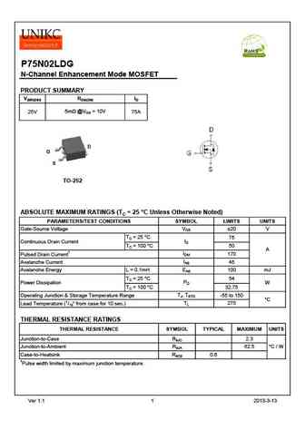
P75N02LDG N-Channel Enhancement Mode MOSFET PRODUCT SUMMARY V(BR)DSS RDS(ON) ID 5m @VGS = 10V 25V 75A TO-252 ABSOLUTE MAXIMUM RATINGS (TC = 25 C Unless Otherwise Noted) PARAMETERS/TEST CONDITIONS SYMBOL LIMITS UNITS VGS Gate-Source Voltage 20 V TC = 25 C 75 ID Continuous Drain Current TC = 100 C 50 A IDM 170 Pulsed Drain Current1 IAS Avalanche Current 45 E
9.1. Size:759K 1
wfp75n08.pdf
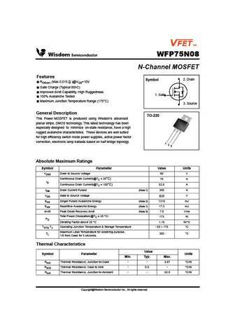
Wisdom Semiconductor WFP75N08 N-Channel MOSFET Features 2. Drain Symbol RDS(on) (Max 0.015 )@VGS=10V Gate Charge (Typical 80nC) Improved dv/dt Capability, High Ruggedness 1. Gate 100% Avalanche Tested Maximum Junction Temperature Range (175 C) 3. Source General Description TO-220 This Power
9.2. Size:72K 1
sup75n06-08 sub75n06-08.pdf
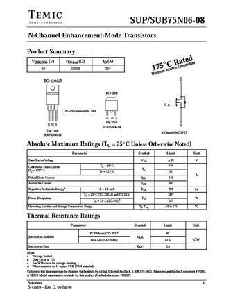
SUP/SUB75N06-08 N-Channel Enhancement-Mode Transistors Product Summary V(BR)DSS (V) rDS(on) (W) ID (A) 60 0.008 75a D TO-220AB TO-263 G DRAIN connected to TAB G D S Top View G D S S SUB75N06-08 Top View N-Channel MOSFET SUP75N06-08 Absolute Maximum Ratings (TC = 25_C Unless Otherwise Noted) Parameter Symbol Limit Unit Gate-Source Voltage VGS "20 V TC = 25_C 75a Continuous
9.3. Size:204K motorola
mtp75n03hdl.pdf

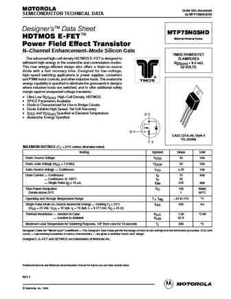
MOTOROLA Order this document SEMICONDUCTOR TECHNICAL DATA by MTP75N03HDL/D Advanced Information MTP75N03HDL HDTMOS E-FET Motorola Preferred Device High Density Power FET N Channel Enhancement Mode Silicon Gate TMOS POWER FET LOGIC LEVEL This advanced high cell density HDTMOS E FET is designed to 75 AMPERES withstand high energy in the avalanche and commutation modes. R
9.4. Size:214K motorola
mtp75n05hd.pdf
MOTOROLA Order this document SEMICONDUCTOR TECHNICAL DATA by MTP75N05HD/D Designer's Data Sheet MTP75N05HD HDTMOS E-FET Motorola Preferred Device Power Field Effect Transistor N Channel Enhancement Mode Silicon Gate TMOS POWER FET This advanced high cell density HDTMOS E FET is designed to 75 AMPERES withstand high energy in the avalanche and commutation modes. RDS
9.5. Size:275K motorola
mtp75n06hd.pdf
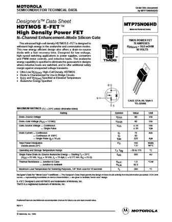
MOTOROLA Order this document SEMICONDUCTOR TECHNICAL DATA by MTP75N06HD/D Designer's Data Sheet MTP75N06HD HDTMOS E-FET Motorola Preferred Device High Density Power FET N Channel Enhancement Mode Silicon Gate TMOS POWER FET This advanced high cell density HDTMOS E FET is designed to 75 AMPERES withstand high energy in the avalanche and commutation modes. RDS(on) = 10.0
9.6. Size:235K motorola
mtp75n03hd.pdf
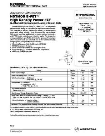
MOTOROLA Order this document SEMICONDUCTOR TECHNICAL DATA by MTP75N03HDL/D Advanced Information MTP75N03HDL HDTMOS E-FET Motorola Preferred Device High Density Power FET N Channel Enhancement Mode Silicon Gate TMOS POWER FET LOGIC LEVEL This advanced high cell density HDTMOS E FET is designed to 75 AMPERES withstand high energy in the avalanche and commutation modes. R
9.7. Size:112K renesas
np75n04yuk.pdf
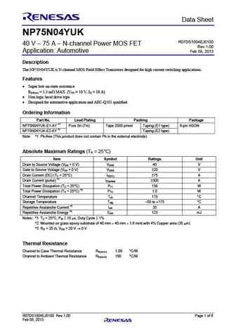
Preliminary Data Sheet NP75N04YUK R07DS1004EJ0100 40 V 75 A N-channel Power MOS FET Rev.1.00 Application Automotive Feb 08, 2013 Description The NP75N04YUK is N-channel MOS Field Effect Transistors designed for high current switching applications. Features Super low on-state resistance RDS(on) = 3.3 m MAX. (VGS = 10 V, ID = 38 A) Non logic level drive typ
9.8. Size:222K renesas
np75n04yug.pdf
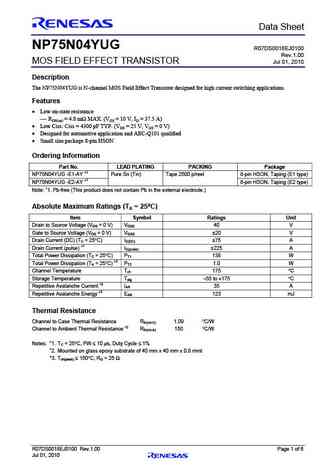
Preliminary Data Sheet NP75N04YUG R07DS0018EJ0100 Rev.1.00 MOS FIELD EFFECT TRANSISTOR Jul 01, 2010 Description The NP75N04YUG is N-channel MOS Field Effect Transistor designed for high current switching applications. Features Low on-state resistance RDS(on) = 4.8 m MAX. (VGS = 10 V, ID = 37.5 A) Low Ciss Ciss = 4300 pF TYP. (VDS = 25 V, VGS = 0 V) Designe
9.9. Size:105K renesas
np75n04vdk.pdf
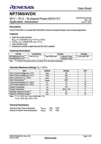
Preliminary Data Sheet NP75N04VDK R07DS1015EJ0100 40 V 75 A N-channel Power MOS FET Rev.1.00 Application Automotive Feb 21, 2013 Description The NP75N04VDK is N-channel MOS Field Effect Transistors designed for high current switching applications. Features Super low on-state resistance RDS(on) = 5.7 m MAX. (VGS = 10 V, ID = 38 A) Low Ciss Ciss = 1630 pF
9.10. Size:112K renesas
np75n055yuk.pdf

Preliminary Data Sheet NP75N055YUK R07DS1005EJ0100 55 V 75 A N-channel Power MOS FET Rev.1.00 Application Automotive Feb 08, 2013 Description The NP75N055YUK is N-channel MOS Field Effect Transistors designed for high current switching applications. Features Super low on-state resistance RDS(on) = 4.5 m MAX. (VGS = 10 V, ID = 38 A) Non logic level drive t
9.11. Size:92K renesas
np75n04vuk.pdf
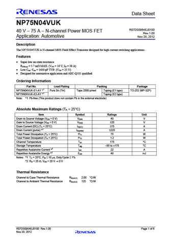
Preliminary Data Sheet NP75N04VUK R07DS0954EJ0100 40 V 75 A N-channel Power MOS FET Rev.1.00 Application Automotive Nov 20, 2012 Description The NP75N04VUK is N-channel MOS Field Effect Transistor designed for high current switching applications. Features Super low on-state resistance RDS(on) = 5.7 m MAX. (VGS = 10 V, ID = 38 A) Low Ciss Ciss = 1630 pF T
9.12. Size:626K fairchild semi
fdp75n08 fdp75n08a.pdf
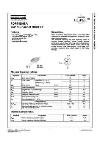
July 2006 TM UniFET FDP75N08A 75V N-Channel MOSFET Features Description 75A, 75V, RDS(on) = 0.011 @VGS = 10 V These N-Channel enhancement mode power field effect Low gate charge ( typical 145nC) transistors are produced using Fairchild s proprietary, planar stripe, DMOS technology. Low Crss ( typical 86pF) This advanced technology has been especially tailored to
9.13. Size:67K vishay
sup75n03-07 sub75n03-07.pdf
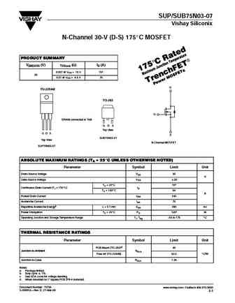
SUP/SUB75N03-07 Vishay Siliconix N-Channel 30-V (D-S) 175_C MOSFET PRODUCT SUMMARY V(BR)DSS (V) rDS(on) (W) ID (A) 0.007 @ VGS = 10 V 75a 30 30 0.01 @ VGS = 4.5 V 70 D TO-220AB TO-263 G DRAIN connected to TAB G D S Top View G D S S SUB75N03-07 Top View N-Channel MOSFET SUP75N03-07 ABSOLUTE MAXIMUM RATINGS (TA = 25_C UNLESS OTHERWISE NOTED) Parameter Symbol Limit Unit Dra
9.14. Size:74K vishay
sup75n05-06 sub75n05-06.pdf
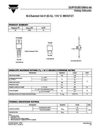
SUP/SUB75N05-06 Vishay Siliconix N-Channel 50-V (D-S), 175_C MOSFET PRODUCT SUMMARY V(BR)DSS (V) rDS(on) (W) ID (A) 50 0.006 75 D TO-220AB TO-263 G DRAIN connected to TAB G D S Top View G D S S SUB75N05-06 Top View N-Channel MOSFET SUP75N05-06 ABSOLUTE MAXIMUM RATINGS (TC = 25_C UNLESS OTHERWISE NOTED) Parameter Symbol Limit Unit Gate-Source Voltage VGS "20 V TC = 25_C 75a
9.15. Size:69K vishay
sup75n03-04.pdf
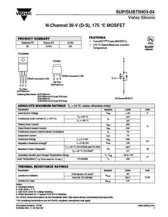
SUP/SUB75N03-04 Vishay Siliconix N-Channel 30-V (D-S), 175 C MOSFET FEATURES PRODUCT SUMMARY TrenchFET Power MOSFETs V(BR)DSS (V) rDS(on) ( )ID (A) Available 175 C Rated Maximum Junction 30 0.004 75a RoHS* Temperature COMPLIANT TO-220AB D TO-263 DRAIN connected to TAB G DRAIN connected to TAB G D S Top View SUB75N03-04 G D S Top View SUP75N03-04 S Or
9.16. Size:66K vishay
sup75n04-05l sub75n04-05l.pdf
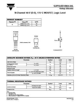
SUP/SUB75N04-05L Vishay Siliconix N-Channel 40-V (D-S), 175_C MOSFET, Logic Level PRODUCT SUMMARY V(BR)DSS (V) rDS(on) (W) ID (A) 0.0055 @ VGS = 10 V 75a 40 0.0065 @ VGS = 4.5 V 75a D TO-220AB TO-263 G DRAIN connected to TAB G D S Top View G D S S SUB75N04-05L Top View N-Channel MOSFET SUP75N04-05L ABSOLUTE MAXIMUM RATINGS (TC = 25_C UNLESS OTHERWISE NOTED) Parameter Symbo
9.17. Size:84K vishay
sup75n08-10 sub75n08-10.pdf
SUP/SUB75N08-10 Vishay Siliconix N-Channel 75-V (D-S), 175_C MOSFET PRODUCT SUMMARY V(BR)DSS (V) rDS(on) (W) ID (A) 75 0.010 75a D TO-220AB TO-263 G DRAIN connected to TAB G D S Top View G D S S SUB75N08-10 Top View N-Channel MOSFET SUP75N08-10 ABSOLUTE MAXIMUM RATINGS (TC = 25_C UNLESS OTHERWISE NOTED) Parameter Symbol Limit Unit Gate-Source Voltage VGS "20 V TC = 25_C 75
9.18. Size:71K vishay
sup75n06-07l sub75n06-07l.pdf
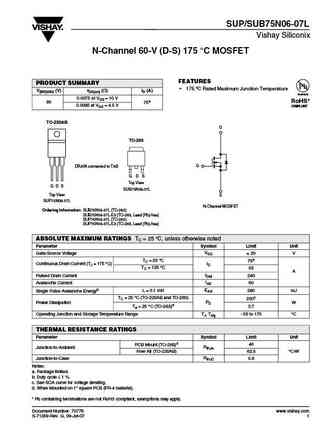
SUP/SUB75N06-07L Vishay Siliconix N-Channel 60-V (D-S) 175 C MOSFET FEATURES PRODUCT SUMMARY 175 C Rated Maximum Junction Temperature V(BR)DSS (V) rDS(on) ( )ID (A) Available 0.0075 at VGS = 10 V RoHS* 60 75a 0.0085 at VGS = 4.5 V COMPLIANT TO-220AB D TO-263 DRAIN connected to TAB G G D S Top View G D S SUB75N06-07L Top View S SUP75N06-07L N-Channel MOSFET
9.19. Size:72K vishay
sup75n05-06a sub75n05-06a.pdf
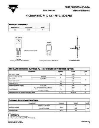
SUP/SUB75N05-06A New Product Vishay Siliconix N-Channel 50-V (D-S), 175_C MOSFET PRODUCT SUMMARY V(BR)DSS (V) rDS(on) (W) ID (A) 50 0.006 75 D TO-220AB TO-263 G DRAIN connected to TAB G D S Top View G D S S Top View N-Channel MOSFET Ordering Information SUP75N05-06A Ordering Information SUB75N05-06A ABSOLUTE MAXIMUM RATINGS (TC = 25_C UNLESS OTHERWISE NOTED) Parameter Symb
9.20. Size:88K vishay
sub75n06-07l sup75n06-07l.pdf

SUP/SUB75N06-07L Vishay Siliconix N-Channel 60-V (D-S) 175 C MOSFET FEATURES PRODUCT SUMMARY 175 C Rated Maximum Junction Temperature V(BR)DSS (V) rDS(on) ( )ID (A) Available 0.0075 at VGS = 10 V RoHS* 60 75a 0.0085 at VGS = 4.5 V COMPLIANT TO-220AB D TO-263 DRAIN connected to TAB G G D S Top View G D S SUB75N06-07L Top View S SUP75N06-07L N-Channel MOSFET
9.21. Size:106K vishay
sup75n05-07 sub75n05-07.pdf
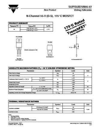
SUP/SUB75N05-07 New Product Vishay Siliconix N-Channel 55-V (D-S), 175_C MOSFET PRODUCT SUMMARY V(BR)DSS (V) rDS(on) (W) ID (A) 0.007 @ VGS = 10 V a 55 "75 a 55 "75 0.009 @ VGS = 4.5 V D TO-220AB TO-263 G DRAIN connected to TAB G D S Top View G D S S SUB75N05-07 Top View N-Channel MOSFET SUP75N05-07 ABSOLUTE MAXIMUM RATINGS (TC = 25_C UNLESS OTHERWISE NOTED) Parameter S
9.22. Size:106K vishay
sup75n08-09l sub75n08-09l.pdf
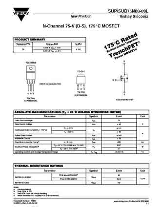
SUP/SUB75N08-09L New Product Vishay Siliconix N-Channel 75-V (D-S), 175_C MOSFET PRODUCT SUMMARY V(BR)DSS (V) rDS(on) (W) ID (A) 0.009 @ VGS = 10 V 75 "75 a 75 "75 a 0.011 @ VGS = 4.5 V D TO-220AB TO-263 G DRAIN connected to TAB G D S Top View G D S S SUB75N08-09L Top View N-Channel MOSFET SUP75N08-09L ABSOLUTE MAXIMUM RATINGS (TC = 25_C UNLESS OTHERWISE NOTED) Parameter
9.23. Size:102K vishay
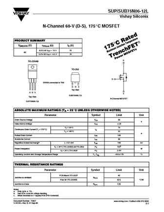
sup75n06-12l sub75n06-12l.pdf
SUP/SUB75N06-12L Vishay Siliconix N-Channel 60-V (D-S), 175_C MOSFET PRODUCT SUMMARY V(BR)DSS (V) rDS(on) (W) ID (A) 0.012 @ VGS = 10 V 75 60 60 0.014 @ VGS = 4.5 V 70 D TO-220AB TO-263 G DRAIN connected to TAB G D S Top View G D S S SUB75N06-12L Top View N-Channel MOSFET SUP75N06-12L ABSOLUTE MAXIMUM RATINGS (TA = 25_C UNLESS OTHERWISE NOTED) Parameter Symbol Limit Unit
9.24. Size:73K vishay
sup75n06-08 sub75n06-08.pdf
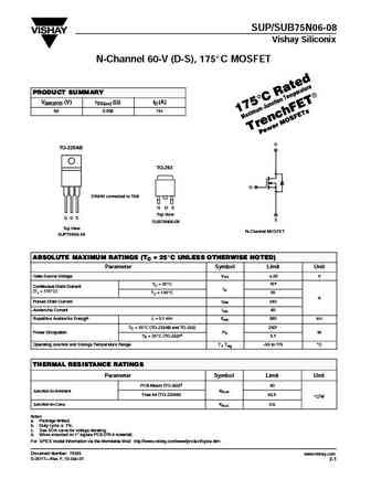
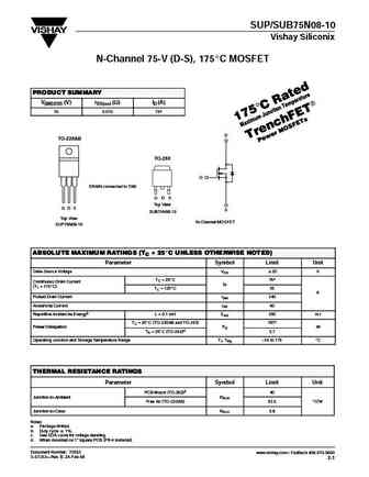
SUP/SUB75N06-08 Vishay Siliconix N-Channel 60-V (D-S), 175_C MOSFET PRODUCT SUMMARY V(BR)DSS (V) rDS(on) (W) ID (A) 60 0.008 75a D TO-220AB TO-263 G DRAIN connected to TAB G D S Top View G D S S SUB75N06-08 Top View N-Channel MOSFET SUP75N06-08 ABSOLUTE MAXIMUM RATINGS (TC = 25_C UNLESS OTHERWISE NOTED) Parameter Symbol Limit Unit Gate-Source Voltage VGS "20 V TC = 25_C 75
9.25. Size:74K onsemi
ntb75n03-006 ntp75n03-06 ntb75n03-06 ntp75n03-6g.pdf
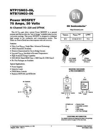
NTP75N03-06, NTB75N03-06 Power MOSFET 75 Amps, 30 Volts N-Channel TO-220 and D2PAK http //onsemi.com This 20 VGS gate drive vertical Power MOSFET is a general purpose part that provides the best of design available today in a low V(BR)DSS RDS(on) TYP ID MAX cost power package. This power MOSFET is designed to withstand high energy in the avalanche and commutation modes. The 30
9.26. Size:79K onsemi
ntb75n06g ntp75n06 ntp75n06 ntb75n06.pdf
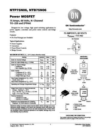
NTP75N06, NTB75N06 Power MOSFET 75 Amps, 60 Volts, N-Channel TO-220 and D2PAK Designed for low voltage, high speed switching applications in http //onsemi.com power supplies, converters and power motor controls and bridge circuits. 75 AMPERES, 60 VOLTS Features RDS(on) = 9.5 mW Pb-Free Packages are Available N-Channel D Typical Applications Power Supplies Converters
9.27. Size:1266K onsemi
fdp75n08a.pdf

Is Now Part of To learn more about ON Semiconductor, please visit our website at www.onsemi.com Please note As part of the Fairchild Semiconductor integration, some of the Fairchild orderable part numbers will need to change in order to meet ON Semiconductor s system requirements. Since the ON Semiconductor product management systems do not have the ability to manage part nomenclatur
9.28. Size:91K onsemi
ntb75n03r ntb75n03r ntp75n03r ntp75n03r.pdf
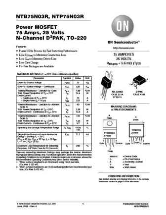
NTB75N03R, NTP75N03R Power MOSFET 75 Amps, 25 Volts N-Channel D2PAK, TO-220 Features http //onsemi.com Planar HD3e Process for Fast Switching Performance 75 AMPERES Low RDS(on) to Minimize Conduction Loss Low Ciss to Minimize Driver Loss 25 VOLTS Low Gate Charge RDS(on) = 5.6 mW (Typ) Pb-Free Packages are Available 4 MAXIMUM RATINGS (TJ = 25 C Unless otherwis
9.29. Size:79K onsemi
ntb75n06l ntp75n06l ntp75n06l ntb75n06l.pdf
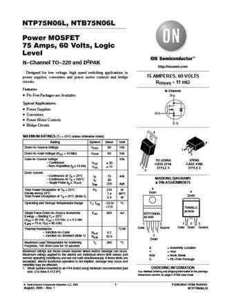
NTP75N06L, NTB75N06L Power MOSFET 75 Amps, 60 Volts, Logic Level N-Channel TO-220 and D2PAK http //onsemi.com Designed for low voltage, high speed switching applications in 75 AMPERES, 60 VOLTS power supplies, converters and power motor controls and bridge circuits. RDS(on) = 11 mW Features N-Channel Pb-Free Packages are Available D Typical Applications Power Supplies G
9.30. Size:72K onsemi
ntb75n03l09t4 ntp75n03l09 ntp75n03l09 ntb75n03l09.pdf
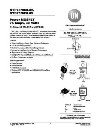
NTP75N03L09, NTB75N03L09 Power MOSFET 75 Amps, 30 Volts N-Channel TO-220 and D2PAK http //onsemi.com This Logic Level Vertical Power MOSFET is a general purpose part 75 AMPERES, 30 VOLTS that provides the best of design available today in a low cost power package. Avalanche energy issues make this part an ideal design in. RDS(on) = 8 mW The drain-to-source diode has a ideal fas
9.31. Size:105K general semi
gfp75n03.pdf
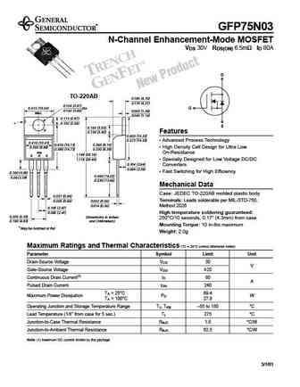
GFP75N03 N-Channel Enhancement-Mode MOSFET V 30V R 6.5m I 80A DS DS(ON) D D TO-220AB 0.185 (4.70) 0.170 (4.31) 0.154 (3.91) Dia. 0.415 (10.54) G 0.142 (3.60) 0.055 (1.39) Max. 0.045 (1.14) 0.113 (2.87) 0.102 (2.56) * S 0.155 (3.93) D 0.134 (3.40) Features 0.603 (15.32) 0.573 (14.55) Advanced Process Technology 0.410 (10.41) 0.635 (16.13) 0.360 (9.14) 0.350 (8.89
9.32. Size:324K cet
cep75n06 ceb75n06.pdf
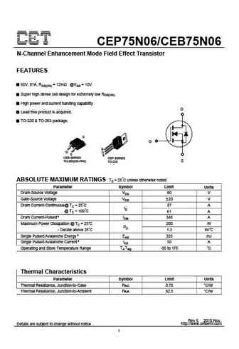
CEP75N06/CEB75N06 N-Channel Enhancement Mode Field Effect Transistor FEATURES 60V, 87A, RDS(ON) = 12m @VGS = 10V. Super high dense cell design for extremely low RDS(ON). High power and current handing capability. D Lead free product is acquired. TO-220 & TO-263 package. G CEB SERIES CEP SERIES TO-263(DD-PAK) S TO-220 ABSOLUTE MAXIMUM RATINGS Tc = 25 C unless otherwise noted Pa
9.33. Size:418K cet
cep75n06g ceb75n06g.pdf
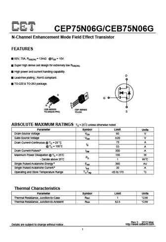
CEP75N06G/CEB75N06G N-Channel Enhancement Mode Field Effect Transistor FEATURES 60V, 75A, RDS(ON) = 13m @VGS = 10V. Super high dense cell design for extremely low RDS(ON). High power and current handing capability. D Lead-free plating ; RoHS compliant. TO-220 & TO-263 package. G CEB SERIES CEP SERIES TO-263(DD-PAK) S TO-220 ABSOLUTE MAXIMUM RATINGS Tc = 25 C unless otherwise no
9.34. Size:93K ape
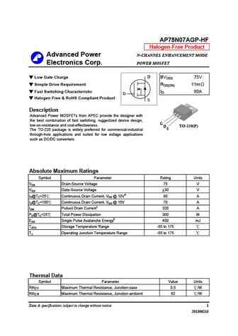
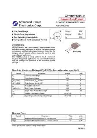
ap75n07agp-hf.pdf
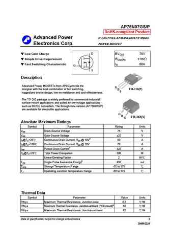
AP75N07AGP-HF Halogen-Free Product Advanced Power N-CHANNEL ENHANCEMENT MODE Electronics Corp. POWER MOSFET D Low Gate Charge BVDSS 75V Simple Drive Requirement RDS(ON) 11m Fast Switching Characteristic ID 80A G Halogen Free & RoHS Compliant Product S Description Advanced Power MOSFETs from APEC provide the designer with the best combination of fast switching, rug
9.35. Size:153K ape
ap75n07agp.pdf
AP75N07AGP-HF Halogen-Free Product Advanced Power N-CHANNEL ENHANCEMENT MODE Electronics Corp. POWER MOSFET D Low Gate Charge BVDSS 75V Simple Drive Requirement RDS(ON) 11m Fast Switching Characteristic ID 80A G Halogen Free & RoHS Compliant Product S Description AP75N07A series are from Advanced Power i
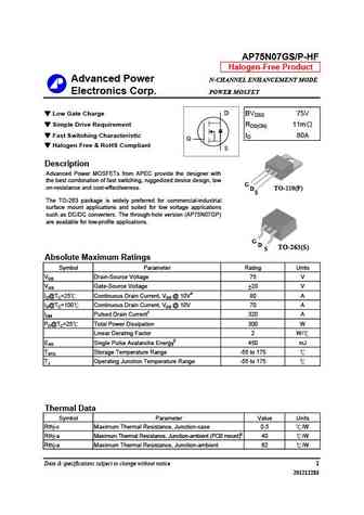
9.36. Size:95K ape
ap75n07gi-hf.pdf
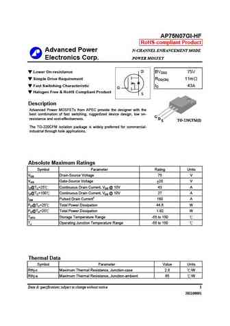
AP75N07GI-HF RoHS-compliant Product Advanced Power N-CHANNEL ENHANCEMENT MODE Electronics Corp. POWER MOSFET D Lower On-resistance BVDSS 75V Simple Drive Requirement RDS(ON) 11m Fast Switching Characteristic ID 43A G Halogen Free & RoHS Compliant Product S Description Advanced Power MOSFETs from APEC provide the designer with the best combination of fast switching
9.37. Size:126K ape
ap75n07gw.pdf
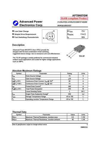
AP75N07GW RoHS-compliant Product Advanced Power N-CHANNEL ENHANCEMENT MODE Electronics Corp. POWER MOSFET D Low Gate Charge BVDSS 75V Simple Drive Requirement RDS(ON) 11m Fast Switching Characteristic ID 90A G S Description Advanced Power MOSFETs from APEC provide the designer with the best combination of fast switching, ruggedized device design, low on-resistance and
9.38. Size:152K ape
ap75n07gp.pdf
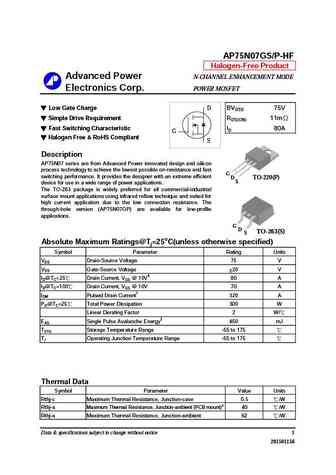
AP75N07GS/P-HF Halogen-Free Product Advanced Power N-CHANNEL ENHANCEMENT MODE Electronics Corp. POWER MOSFET D Low Gate Charge BVDSS 75V Simple Drive Requirement RDS(ON) 11m Fast Switching Characteristic ID 80A G Halogen Free & RoHS Compliant S Description AP75N07 series are from Advanced Power innovated
9.39. Size:192K ape
ap75n07gs p.pdf
AP75N07GS/P RoHS-compliant Product Advanced Power N-CHANNEL ENHANCEMENT MODE Electronics Corp. POWER MOSFET D Low Gate Charge BVDSS 75V Simple Drive Requirement RDS(ON) 11m Fast Switching Characteristic ID 80A G S Description Advanced Power MOSFETs from APEC provide the G designer with the best combination of fast switching, TO-220(P) D S ruggedized device design,
9.40. Size:165K ape
ap75n07gs.pdf

AP75N07GS/P-HF Halogen-Free Product Advanced Power N-CHANNEL ENHANCEMENT MODE Electronics Corp. POWER MOSFET D Low Gate Charge BVDSS 75V Simple Drive Requirement RDS(ON) 11m Fast Switching Characteristic ID 80A G Halogen Free & RoHS Compliant S Description AP75N07 series are from Advanced Power innovated
9.41. Size:97K ape
ap75n07gsp-hf.pdf
AP75N07GS/P-HF Halogen-Free Product Advanced Power N-CHANNEL ENHANCEMENT MODE Electronics Corp. POWER MOSFET D Low Gate Charge BVDSS 75V Simple Drive Requirement RDS(ON) 11m Fast Switching Characteristic ID 80A G Halogen Free & RoHS Compliant S Description Advanced Power MOSFETs from APEC provide the designer with the best combination of fast switching, ruggedized
9.42. Size:270K shantou-huashan
hfp75n08.pdf
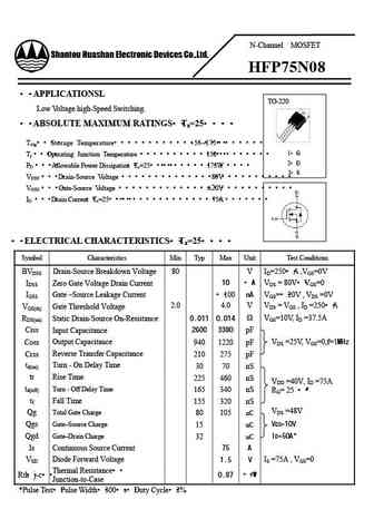
N-Channel MOSFET Shantou Huashan Electronic Devices Co.,Ltd. HFP75N08 APPLICATIONSL TO-220 Low Voltage high-Speed Switching. ABSOLUTE MAXIMUM RATINGS Ta=25 Tstg Storage Temperature -55 175 1 G Tj Operating Junction Temperature 150 2 D PD Allowable Power Dissipation
9.43. Size:143K tysemi
kup75n08.pdf
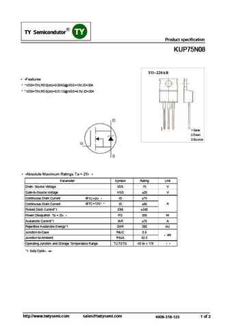
SMDType IC DIP Type MOSFET Product specification KUP 75N08 Features VDS=75V,RDS(on)=0.009 @VGS=10V,ID=30A VDS=75V,RDS(on)=0.011 @VGS=4.5V,ID=20A 1 Gate 2 Drain 3 Source Absolute Maximum Ratings Ta = 25 Parameter Symbol Rating Unit Drain- Source Voltage VDS 75 V Gate-to-Source Voltage VGS 20 V ID 75 Continuous Drain Current @TC 25 = @TC
9.44. Size:1259K winsemi
sfp75n08r.pdf
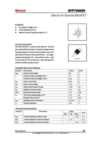
SFP75N08R SFP75N08R SFP75N08R SFP75N08R Silicon N-Channel MOSFET Silicon N-Channel MOSFET Silicon N-Channel MOSFET Silicon N-Channel MOSFET Features R (Max0.015 )@V =10v DS(on) GS Gate Charge(Typical 80 nC) Maximum Junction Temperature Range(175 ) General Description This Power MOSFET is produced using Winsemi s advanced planar stripe,DMOS technology. This lates
9.46. Size:750K cn vbsemi
sup75n08-10.pdf
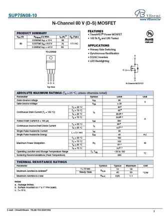
SUP75N08-10 www.VBsemi.tw N-Channel 80 V (D-S) MOSFET FEATURES PRODUCT SUMMARY TrenchFET Power MOSFET a VDS (V) RDS(on) ( ) Max. ID (A) Qg (Typ.) 100 % Rg and UIS Tested 0.0065at VGS = 10 V 80 80 0.0070at VGS = 6.0 V 75 17.1 nC APPLICATIONS 0.0085at VGS = 4.5 V 65 Primary Side Switching TO-220AB Synchronous Rectification D DC/AC Inverters LED Backl
Otros transistores... P0420AI
, P0425AD
, P0425AI
, P7004EM
, P7004EV
, P7006BL
, P7502CMG
, P7503BMG
, AO4468
, PZP003BYB
, PZP103BYB
, TD304BH
, TD357EG
, TD381BA
, TD422BL
, P4506BD
, P4506BV
.