2021 Datasheet. Equivalente. Reemplazo. Hoja de especificaciones. Principales características
Número de Parte: 2021 📄📄
Tipo de FET: MOSFET
Polaridad de transistor: N
ESPECIFICACIONES MÁXIMAS
Pdⓘ - Máxima disipación de potencia: 0.31 W
|Vds|ⓘ - Voltaje máximo drenador-fuente: 20 V
|Vgs|ⓘ - Voltaje máximo fuente-puerta: 6 V
|Id|ⓘ - Corriente continua de drenaje: 0.55 A
Tjⓘ - Temperatura máxima de unión: 150 °C
CARACTERÍSTICAS ELÉCTRICAS
RDSonⓘ - Resistencia estado encendido drenaje a fuente: 0.31 Ohm
Encapsulados: SOT323
📄📄 Copiar
Búsqueda de reemplazo de 2021 MOSFET
- Selecciónⓘ de transistores por parámetros
2021 datasheet
..1. Size:473K shenzhen
2021.pdf 
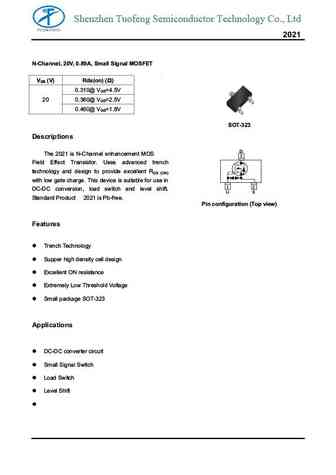
Shenzhen Tuofeng Semiconductor Technology Co., Ltd 2021 N-Channel, 20V, 0.89A, Small Signal MOSFET VDS (V) Rds(on) ( ) 0.310@ VGS=4.5V 20 0.360@ VGS=2.5V 0.460@ VGS=1.8V SOT-323 Descriptions D The 2021 is N-Channel enhancement MOS 3 Field Effect Transistor. Uses advanced trench technology and design to provide excellent RDS (ON) with low gate charge. This device is suitable fo
0.3. Size:66K philips
pssi2021say.pdf
PSSI2021SAY Constant current source in SOT353 package Rev. 03 27 August 2009 Product data sheet 1. Product profile 1.1 General description Resistor-equipped PNP transistor with two diodes on one chip in a SOT353 (SC-88A) plastic package. Stabilized output current of between 15 A and 50 mA by connection of an external resistor between pins 4 and 5. 1.2 Features One chip integrate
0.4. Size:109K philips
pbls2021d.pdf
PBLS2021D 20 V, 1.8 A PNP BISS loadswitch Rev. 02 6 September 2009 Product data sheet 1. Product profile 1.1 General description PNP low VCEsat Breakthrough In Small Signal (BISS) transistor and NPN Resistor- Equipped Transistor (RET) in a SOT457 (SC-74) small Surface-Mounted Device (SMD) plastic package. 1.2 Features Low VCEsat (BISS) and resistor-equipped transistor in one packa
0.5. Size:78K philips
cgy2021g 2.pdf
INTEGRATED CIRCUITS DATA SHEET CGY2021G DCS/PCS 2 W power amplifier 1997 Apr 03 Preliminary specification Supersedes data of 1996 Oct 15 File under Integrated Circuits, IC17 Philips Semiconductors Preliminary specification DCS/PCS 2 W power amplifier CGY2021G FEATURES GENERAL DESCRIPTION Power Amplifier (PA) overall efficiency 50% (DCS) The CGY2021G is a DCS/PCS class 1 GaAs Mon
0.6. Size:225K nec
nesg2021m16.pdf
NPN SILICON GERMANIUM RF TRANSISTOR NESG2021M16 NPN SiGe RF TRANSISTOR FOR LOW NOISE, HIGH-GAIN AMPLIFICATION 6-PIN LEAD-LESS MINIMOLD (M16, 1208 PKG) FEATURES The device is an ideal choice for low noise, high-gain at low current amplifications NF = 0.9 dB TYP., Ga = 18.0 dB TYP. @ VCE = 2 V, IC = 3 mA, f = 2 GHz NF = 1.3 dB TYP., Ga = 10.0 dB TYP. @ VCE = 2 V, IC = 3 mA, f
0.7. Size:729K nec
nesg2021m05.pdf
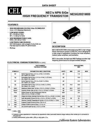
DATA SHEET NEC's NPN SiGe NESG2021M05 HIGH FREQUENCY TRANSISTOR FEATURES HIGH BREAKDOWN VOLTAGE SiGe TECHNOLOGY VCEO = 5 V (Absolute Maximum) LOW NOISE FIGURE NF = 0.9 dB at 2 GHz NF = 1.3 dB at 5.2 GHz HIGH MAXIMUM STABLE GAIN MSG = 22.5 dB at 2 GHz LOW PROFILE M05 PACKAGE M05 SOT-343 footprint, with a height of only 0.59 mm Flat lead style for b
0.8. Size:371K samsung
ssd2021.pdf
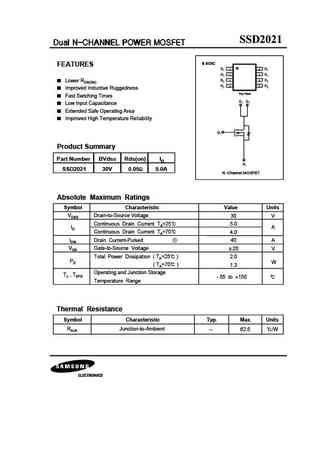
I I I I 8 SOIC FEATURES 8 S1 1 D1 G1 2 7 D1 3 6 S2 D2 Lower RDS(ON) 5 G2 4 D2 Improved Inductive Ruggedness Top View Fast Swtching Times D1 D1 Low Input Capacitance Extended Safe Operating Area Improved High Temperature Reliability G1 Product Summary Part Number BVdss Rds(on) ID S1 SSD2021 30V 0.05 5.0A N -Channel MOSFET Absolute Maximum
0.10. Size:288K diodes
dmp2021ufdf.pdf
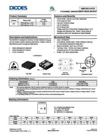
DMP2021UFDF P-CHANNEL ENHANCEMENT MODE MOSFET Product Summary Features and Benefits 0.6mm Profile Ideal for Low Profile Applications ID max V(BR)DSS RDS(ON) max PCB Footprint of 4mm2 TA = +25 C 16m @ VGS = -4.5V -9.0A Low Gate Threshold Voltage -20V -7.7A 22m @ VGS = -2.5V Low On-Resistance ESD protected Gate Totally Lead-Free & Full
0.11. Size:45K panasonic
2sa2021.pdf
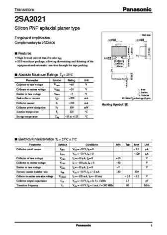
Transistors 2SA2021 Silicon PNP epitaxial planer type Unit mm For general amplification 0.33+0.05 0.10+0.05 0.02 0.02 Complementary to 2SC5609 3 Features High foward current transfer ratio hFE 0.23+0.05 1 2 0.02 (0.40) (0.40) SSS-mini type package, allowing downsizing and thinning of the 0.80 0.05 equipment and automatic insertion through the tape packing 1.2
0.12. Size:225K fuji
2sk2021-01.pdf
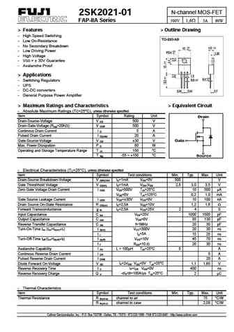
N-channel MOS-FET 2SK2021-01 FAP-IIA Series 500V 1,6 5A 60W > Features > Outline Drawing - High Speed Switching - Low On-Resistance - No Secondary Breakdown - Low Driving Power - High Voltage - VGS = 30V Guarantee - Avalanche Proof > Applications - Switching Regulators - UPS - DC-DC converters - General Purpose Power Amplifier > Maximum Ratings and Characteristics > Equiva
0.13. Size:148K triquint
tgf2021-04.pdf
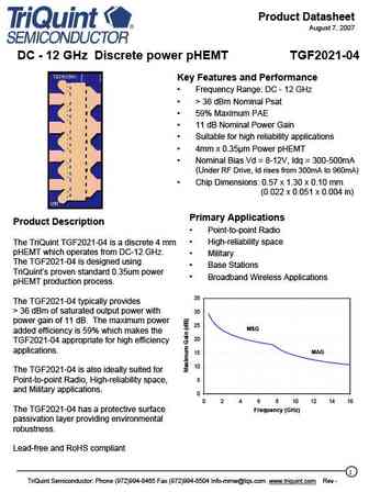
Product Datasheet August 7, 2007 DC - 12 GHz Discrete power pHEMT TGF2021-04 Key Features and Performance Frequency Range DC - 12 GHz > 36 dBm Nominal Psat 59% Maximum PAE 11 dB Nominal Power Gain Suitable for high reliability applications 4mm x 0.35 m Power pHEMT Nominal Bias Vd = 8-12V, Idq = 300-500mA (Under RF Drive, Id rises from 300mA to 960mA)
0.14. Size:145K triquint
tgf2021-08.pdf
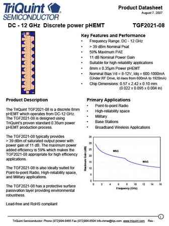
Product Datasheet August 7, 2007 DC - 12 GHz Discrete power pHEMT TGF2021-08 Key Features and Performance Frequency Range DC - 12 GHz > 39 dBm Nominal Psat 59% Maximum PAE 11 dB Nominal Power Gain Suitable for high reliability applications 8mm x 0.35 m Power pHEMT Nominal Bias Vd = 8-12V, Idq = 600-1000mA (Under RF Drive, Id rises from 600mA to 1920mA)
0.15. Size:146K triquint
tgf2021-02.pdf
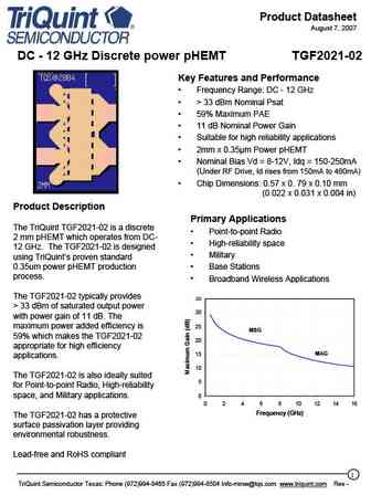
Product Datasheet August 7, 2007 DC - 12 GHz Discrete power pHEMT TGF2021-02 Key Features and Performance Frequency Range DC - 12 GHz > 33 dBm Nominal Psat 59% Maximum PAE 11 dB Nominal Power Gain Suitable for high reliability applications 2mm x 0.35 m Power pHEMT Nominal Bias Vd = 8-12V, Idq = 150-250mA (Under RF Drive, Id rises from 150mA to 480mA)
0.16. Size:153K triquint
tgf2021-12.pdf
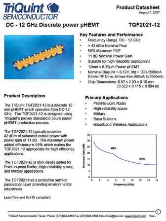
Product Datasheet August 7, 2007 DC - 12 GHz Discrete power pHEMT TGF2021-12 Key Features and Performance Frequency Range DC - 12 GHz > 42 dBm Nominal Psat 58% Maximum PAE 11 dB Nominal Power Gain Suitable for high reliability applications 12mm x 0.35 m Power pHEMT Nominal Bias Vd = 8-12V, Idq = 900-1500mA (Under RF Drive, Id rises from 900mA to 2560mA
0.17. Size:502K willsemi
wnm2021.pdf
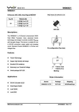
WNM2021 WNM2021 Http //www.sh-willsemi.com N-Channel, 20V, 0.89A, Small Signal MOSFET VDS (V) Rds(on) ( ) 0.220@ VGS=4.5V D 20 0.260@ VGS=2.5V S 0.320@ VGS=1.8V G SOT-323 Descriptions D The WNM2021 is N-Channel enhancement MOS 3 Field Effect Transistor. Uses advanced trench technology and design to provide excellent RDS (ON) with low gate charge. This device is suitable
0.18. Size:269K ruichips
ru2021h.pdf
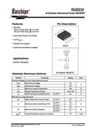
RU2021H N-Channel Advanced Power MOSFET MOSFET Features Pin Description 20V/20A, RDS (ON) =4m (Typ.) @ VGS=10V RDS (ON) =5m (Typ.) @ VGS=4.5V Super High Dense Cell Design Low RDS(ON) Reliable and Rugged SOP-8 Lead Free and Green Available Applications DC/DC Converter N-Channel MOSFET Absolute Maximum Ratings Symbol Parameter Rating Unit Common Rat
0.19. Size:38K sensitron
shd220212 shdc220212.pdf
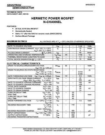
SHD220212 SENSITRON SEMICONDUCTOR TECHNICAL DATA DATA SHEET 4067, REV B HERMETIC POWER MOSFET N-CHANNEL FEATURES 30 Volt, 0.019 Ohm MOSFET Hermetically Sealed Add a C after the SHD for ceramic seals (SHDC220212) Surface Mount Package MAXIMUM RATINGS ALL RATINGS ARE AT TA = 25 C UNLESS OTHERWISE SPECIFIED. RATING SYMBOL MIN. TYP. MAX. UNITS GA
0.20. Size:72K sensitron
shd220213 shdc220213.pdf
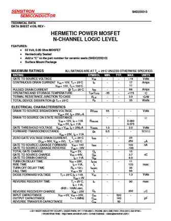
SHD220213 SENSITRON SEMICONDUCTOR TECHNICAL DATA DATA SHEET 4139, REV - HERMETIC POWER MOSFET N-CHANNEL LOGIC LEVEL FEATURES 55 Volt, 0.06 Ohm MOSFET Hermetically Sealed Add a C to the part number for ceramic seals (SHDC220213) Surface Mount Package MAXIMUM RATINGS ALL RATINGS ARE AT TA = 25 C UNLESS OTHERWISE SPECIFIED. RATING SYMBOL MIN. TYP. MAX. UNITS GAT
0.21. Size:431K slkor
wnm2021.pdf
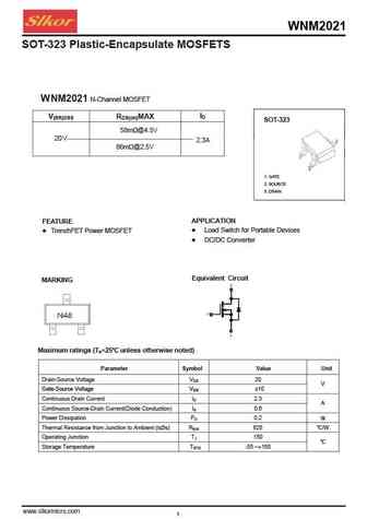
WNM2021 SOT-323 Plastic-Encapsulate MOSFETS W NM2021 N-Channel MOSFET ID V(BR)DSS RDS(on)MAX SOT-323 58m @4.5V 20 V 2.3A @2.5V 86m 1. GATE 2. SOURCE 3. DRAIN APPLICATION FEATURE Load Switch for Portable Devices TrenchFET Power MOSFET DC/DC Converter Equivalent Circuit MARKING Maximum ratings (Ta=25 unless otherwise noted) Parameter Symbol Value
0.22. Size:844K cn vbsemi
wnm2021.pdf
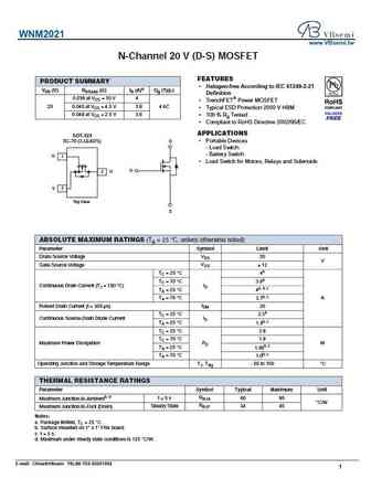
WNM2021 www.VBsemi.tw N-Channel 20 V (D-S) MOSFET FEATURES PRODUCT SUMMARY Halogen-free According to IEC 61249-2-21 VDS (V) RDS(on) ( )ID (A)a Qg (Typ.) Definition 0.036 at VGS = 10 V 4 TrenchFET Power MOSFET 20 0.040 at VGS = 4.5 V 3.8 4 nC Typical ESD Protection 2000 V HBM 0.048 at VGS = 2.5 V 3.6 100 % Rg Tested Compliant to RoHS Directive 2002/95/EC A
0.23. Size:206K inchange semiconductor
mj12021.pdf
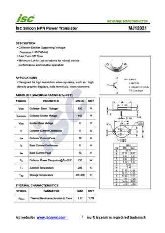
isc Silicon NPN Power Transistor MJ12021 DESCRIPTION Collector-Emitter Sustaining Voltage- V = 450V(Min) CEO(SUS) Fast Turn-Off Time Minimum Lot-to-Lot variations for robust device performance and reliable operation APPLICATIONS Designed for high resolution video systems, such as high density graphic displays, data terminals, video scanners. ABSOLUTE MAXIMUM RATINGS(T =25
0.24. Size:180K inchange semiconductor
2sd2021.pdf
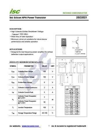
INCHANGE Semiconductor isc Silicon NPN Power Transistor 2SD2021 DESCRIPTION High Collector-Emitter Breakdown Voltage- V = 150V (Min) (BR)CEO Wide Area of Safe Operation Minimum Lot-to-Lot variations for robust device performance and reliable operation APPLICATIONS Designed for low frequency power amplifier TV vertical deflection output applications ABSOLUTE MAXIMUM RATINGS
0.25. Size:215K inchange semiconductor
2sk2021-01.pdf
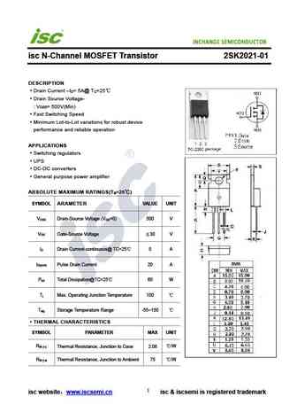
isc N-Channel MOSFET Transistor 2SK2021-01 DESCRIPTION Drain Current I = 5A@ T =25 D C Drain Source Voltage- V = 500V(Min) DSS Fast Switching Speed Minimum Lot-to-Lot variations for robust device performance and reliable operation APPLICATIONS Switching regulators UPS DC-DC converters General purpose power amplifier ABSOLUTE MAXIMUM RATINGS(T =25 ) a S
Otros transistores... APM9984CCG, APM9986CO, APM9988CO, APM9988QA, SIR164DP, 1481, 2015, 2016, AO3400, 2026, 2341, 4401, 4402, 4407, 4409, 4410, 4435