1002 MOSFET Equivalente. Reemplazo. Hoja de especificaciones. Principales características
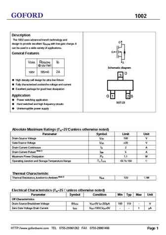
Número de Parte: 1002
Tipo de FET: MOSFET
Polaridad de transistor: N
ESPECIFICACIONES MÁXIMAS
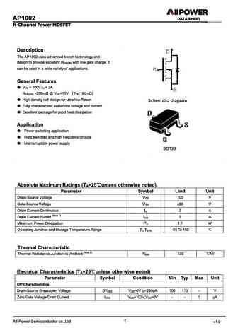
Pdⓘ - Máxima disipación de potencia: 1.1 W
|Vds|ⓘ - Voltaje máximo drenador-fuente: 100 V
|Vgs|ⓘ - Voltaje máximo fuente-puerta: 20 V
|Id|ⓘ - Corriente continua de drenaje: 2 A
Tjⓘ - Temperatura máxima de unión: 150 °C
CARACTERÍSTICAS ELÉCTRICAS
trⓘ - Tiempo de subida: 10 nS
Cossⓘ - Capacitancia de salida: 22 pF
RDSonⓘ - Resistencia estado encendido drenaje a fuente: 0.22 Ohm
Encapsulados: SOT23
Búsqueda de reemplazo de 1002 MOSFET
- Selecciónⓘ de transistores por parámetros
1002 datasheet
mrf1002ma mrf1002mb.pdf
MOTOROLA Order this document SEMICONDUCTOR TECHNICAL DATA by MRF1002MA/D The RF Line Microwave Pulse MRF1002MA Power Transistors MRF1002MB . . . designed for Class B and C common base amplifier applications in short and long pulse TACAN, IFF, DME, and radar transmitters. Guaranteed Performance @ 1090 MHz, 35 Vdc Output Power = 2.0 Watts Peak 2.0 W (PEAK), 960 1215 MHz Minimu
mj10022r.pdf
Order this document MOTOROLA by MJ10022/D SEMICONDUCTOR TECHNICAL DATA MJ10022 MJ10023 Designer's Data Sheet SWITCHMODE Series 40 AMPERE NPN Silicon Power Darlington NPN SILICON POWER DARLINGTON Transistors with Base-Emitter TRANSISTORS 350 AND 400 VOLTS Speedup Diode 250 WATTS The MJ10022 and MJ10023 Darlington transistors are designed for high voltage, high speed, pow
mrf1002m.pdf
MOTOROLA Order this document SEMICONDUCTOR TECHNICAL DATA by MRF1002MA/D The RF Line Microwave Pulse MRF1002MA Power Transistors MRF1002MB . . . designed for Class B and C common base amplifier applications in short and long pulse TACAN, IFF, DME, and radar transmitters. Guaranteed Performance @ 1090 MHz, 35 Vdc Output Power = 2.0 Watts Peak 2.0 W (PEAK), 960 1215 MHz Minimu
mj10020r.pdf
Order this document MOTOROLA by MJ10020/D SEMICONDUCTOR TECHNICAL DATA MJ10020 MJ10021 Designer's Data Sheet SWITCHMODE Series 60 AMPERE NPN Silicon Power Darlington NPN SILICON POWER DARLINGTON Transistors with Base-Emitter TRANSISTORS 200 AND 250 VOLTS Speedup Diode 250 WATTS The MJ10020 and MJ10021 Darlington transistors are designed for high voltage, high speed, pow
msc81002.pdf
MSC81002 RF & MICROWAVE TRANSISTORS GENERAL PURPOSE AMPLIFIER APPLICATIONS .EMITTER BALLASTED .VSWR CAPABILITY 1 @ RATED CONDITIONS .HERMETIC STRIPAC PACKAGE .P 2.0 W MIN. WITH 10 dB GAIN @ OUT = 1 GHz .230 2L STUD (S016) hermetically sealed ORDER CODE BRANDING MSC81002 81002 PIN CONNECTION DESCRIPTION The MSC81002 is a common base hermetically sealed silicon NPN micro
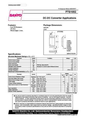
fts1002.pdf
Ordering number EN5887 P-Channel Silicon MOSFET FTS1002 DC-DC Converter Applications Features Package Dimensions Low ON Resistance. unit mm 4V drive. 2147 Mount height 1.1mm. [FTS1002] 3.0 0.975 0.65 8 5 1 Drain 2 Source 3 Source 4 Gate 5 Drain 1 4 6 Source 0.125 0.25 7 Source 8 Drain SANYO TSSOP8 Specifications Absolute Maximum Ratings at Ta = 25 C Par
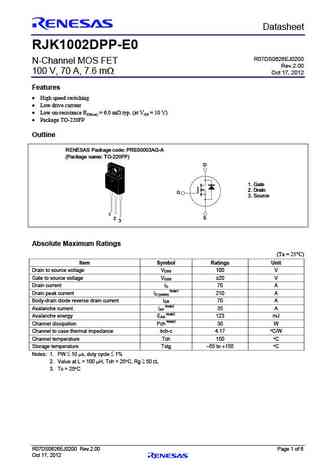
rjk1002dpp-e0.pdf
Preliminary Datasheet RJK1002DPP-E0 R07DS0626EJ0200 N-Channel MOS FET Rev.2.00 100 V, 70 A, 7.6 m Oct 17, 2012 Features High speed switching Low drive current Low on-resistance RDS(on) = 6.0 m typ. (at VGS = 10 V) Package TO-220FP Outline RENESAS Package code PRSS0003AG-A (Package name TO-220FP) D 1. Gate 2. Drain G 3. Source 1 S 2 3 Ab
rej03g1002 2sk2202ds.pdf
To our customers, Old Company Name in Catalogs and Other Documents On April 1st, 2010, NEC Electronics Corporation merged with Renesas Technology Corporation, and Renesas Electronics Corporation took over all the business of both companies. Therefore, although the old company name remains in this document, it is a valid Renesas Electronics document. We appreciate your understanding.
rej03g1131 h7n1002ldlslmds.pdf
To our customers, Old Company Name in Catalogs and Other Documents On April 1st, 2010, NEC Electronics Corporation merged with Renesas Technology Corporation, and Renesas Electronics Corporation took over all the business of both companies. Therefore, although the old company name remains in this document, it is a valid Renesas Electronics document. We appreciate your understanding.
h7n1002lm.pdf
To our customers, Old Company Name in Catalogs and Other Documents On April 1st, 2010, NEC Electronics Corporation merged with Renesas Technology Corporation, and Renesas Electronics Corporation took over all the business of both companies. Therefore, although the old company name remains in this document, it is a valid Renesas Electronics document. We appreciate your understanding.
rej03g1601 h7p1002dldsds.pdf
To our customers, Old Company Name in Catalogs and Other Documents On April 1st, 2010, NEC Electronics Corporation merged with Renesas Technology Corporation, and Renesas Electronics Corporation took over all the business of both companies. Therefore, although the old company name remains in this document, it is a valid Renesas Electronics document. We appreciate your understanding.
haf1002l haf1002s.pdf
To our customers, Old Company Name in Catalogs and Other Documents On April 1st, 2010, NEC Electronics Corporation merged with Renesas Technology Corporation, and Renesas Electronics Corporation took over all the business of both companies. Therefore, although the old company name remains in this document, it is a valid Renesas Electronics document. We appreciate your understanding.
rej03g0130 h7n1002ab.pdf
To our customers, Old Company Name in Catalogs and Other Documents On April 1st, 2010, NEC Electronics Corporation merged with Renesas Technology Corporation, and Renesas Electronics Corporation took over all the business of both companies. Therefore, although the old company name remains in this document, it is a valid Renesas Electronics document. We appreciate your understanding.
rej03g0660 2sb1002ds-1.pdf
To our customers, Old Company Name in Catalogs and Other Documents On April 1st, 2010, NEC Electronics Corporation merged with Renesas Technology Corporation, and Renesas Electronics Corporation took over all the business of both companies. Therefore, although the old company name remains in this document, it is a valid Renesas Electronics document. We appreciate your understanding.
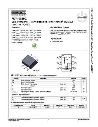
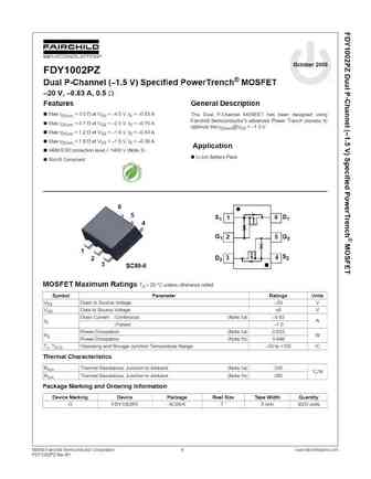
fdy1002pz.pdf
October 2008 FDY1002PZ Dual P-Channel ( 1.5 V) Specified PowerTrench MOSFET 20 V, 0.83 A, 0.5 Features General Description Max rDS(on) = 0.5 at VGS = 4.5 V, ID = 0.83 A This Dual P-Channel MOSFET has been designed using Fairchild Semiconductor s advanced Power Trench process to Max rDS(on) = 0.7 at VGS = 2.5 V, ID = 0.70 A optimize the rDS(on)@VG
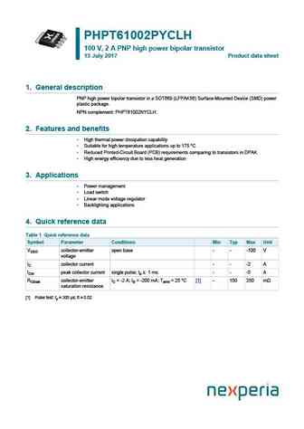
phpt61002pyclh.pdf
PHPT61002PYCLH 100 V, 2 A PNP high power bipolar transistor 13 July 2017 Product data sheet 1. General description PNP high power bipolar transistor in a SOT669 (LFPAK56) Surface-Mounted Device (SMD) power plastic package. NPN complement PHPT61002NYCLH. 2. Features and benefits High thermal power dissipation capability Suitable for high temperature applications up to 175 C
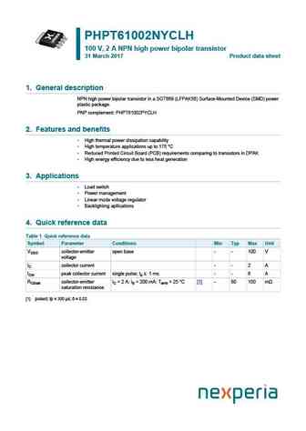
phpt61002nyclh.pdf
PHPT61002NYCLH 100 V, 2 A NPN high power bipolar transistor 31 March 2017 Product data sheet 1. General description NPN high power bipolar transistor in a SOT669 (LFPAK56) Surface-Mounted Device (SMD) power plastic package. PNP complement PHPT61002PYCLH 2. Features and benefits High thermal power dissipation capability High temperature applications up to 175 C Reduced P
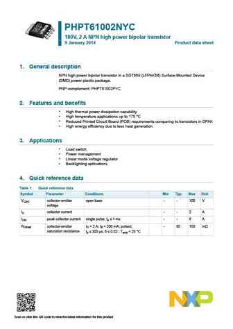
phpt61002nyc.pdf
PHPT61002NYC 100V, 2 A NPN high power bipolar transistor 9 January 2014 Product data sheet 1. General description NPN high power bipolar transistor in a SOT669 (LFPAK56) Surface-Mounted Device (SMD) power plastic package. PNP complement PHPT61002PYC 2. Features and benefits High thermal power dissipation capability High temperature applications up to 175 C Reduced Print
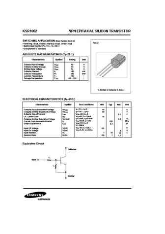
ksr1002.pdf
KSR1002 NPN EPITAXIAL SILICON TRANSISTOR SWITCHING APPLICATION (Bias Resistor Built In) TO-92 Switching circuit, Inverter, Interface circuit, Driver Circuit Built in bias Resistor (R1=10 , R2=10 ) Complement to KSR2002 ABSOLUTE MAXIMUM RATINGS (T =25 ) A Characteristic Symbol Rating Unit Collector-Base Voltage VCBO 50 V Collector-Emitter Voltage VCEO 50 V Emitter-Base Vo
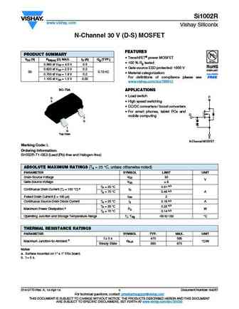
si1002r.pdf
Si1002R www.vishay.com Vishay Siliconix N-Channel 30 V (D-S) MOSFET FEATURES PRODUCT SUMMARY TrenchFET power MOSFET VDS (V) RDS(on) ( ) MAX. ID (A) Qg (TYP.) 100 % Rg tested 0.560 at VGS = 4.5 V 0.5 Gate-source ESD protected 1000 V 0.620 at VGS = 2.5 V 0.2 30 0.72 nC Material categorization 0.700 at VGS = 1.8 V 0.2 For definitions of compliance please see 1.
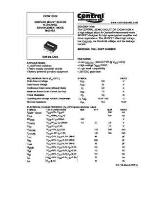
cxdm1002n.pdf
CXDM1002N SURFACE MOUNT SILICON www.centralsemi.com N-CHANNEL DESCRIPTION ENHANCEMENT-MODE The CENTRAL SEMICONDUCTOR CXDM1002N is MOSFET a high voltage silicon N-Channel enhancement-mode MOSFET designed for high speed pulsed amplifier and driver applications. This MOSFET offers high voltage, low rDS(ON), low threshold voltage, and low leakage current. MARKING FULL PART NUMBE
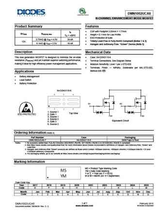
dmn1002uca6.pdf
DMN1002UCA6 N-CHANNEL ENHANCEMENT MODE MOSFET Product Summary Features CSP with Footprint 3.05mm 1.77mm IS BVSSS RSS(ON) Max Height = 0.11mm for Low Profile TA = +25 C ESD Protection of Gate 2.75m @ VGS = 4.5V 24.4A Totally Lead-Free & Fully RoHS Compliant (Notes 1 & 2) 12V 6.1m @ VGS = 2.5V 16.4A Halogen and Antimony Free. Green D
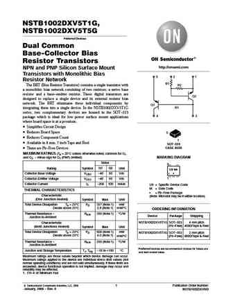
nstb1002dxv5.pdf
NSTB1002DXV5T1G, NSTB1002DXV5T5G Preferred Devices Dual Common Base-Collector Bias Resistor Transistors http //onsemi.com NPN and PNP Silicon Surface Mount Transistors with Monolithic Bias 31 2 Resistor Network R1 The BRT (Bias Resistor Transistor) contains a single transistor with R2 a monolithic bias network consisting of two resistors; a series base resistor and a base-emitter
nstb1002dxv5-d.pdf
NSTB1002DXV5T1G, NSTB1002DXV5T5G Preferred Devices Dual Common Base-Collector Bias Resistor Transistors http //onsemi.com NPN and PNP Silicon Surface Mount Transistors with Monolithic Bias 31 2 Resistor Network R1 The BRT (Bias Resistor Transistor) contains a single transistor with R2 a monolithic bias network consisting of two resistors; a series base resistor and a base-emitter
fdy1002pz.pdf
2021/8/6 FAIR-S-A0002366002-1.pdf https //rocelec.widen.net/view/pdf/ndq325fhpn/FAIR-S-A0002366002-1.pdf?t.download=true&u=5oefqw 1/7 2021/8/6 FAIR-S-A0002366002-1.pdf https //rocelec.widen.net/view/pdf/ndq325fhpn/FAIR-S-A0002366002-1.pdf?t.download=true&u=5oefqw 2/7 2021/8/6 FAIR-S-A0002366002-1.pdf https //rocelec.widen.net/view/pdf/ndq325fhpn/FAIR-S-A0002366002-1.pdf?t.download=true&u
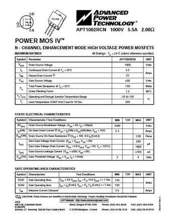
apt1002rcn.pdf
D TO-254 G APT1002RCN 1000V 5.5A 2.00 S TM POWER MOS IV N - CHANNEL ENHANCEMENT MODE HIGH VOLTAGE POWER MOSFETS MAXIMUM RATINGS All Ratings TC = 25 C unless otherwise specified. Symbol Parameter APT1002RCN UNIT VDSS Drain-Source Voltage 1000 Volts ID Continuous Drain Current @ TC = 25 C 5.5 Amps IDM Pulsed Drain Current 1 22 VGS Gate-Source Voltage 30 Volts Total Powe
apt10021jll.pdf
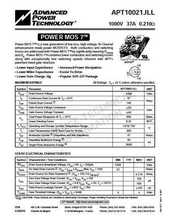
APT10021JLL 1000V 37A 0.210W TM POWER MOS 7 Power MOS 7TM is a new generation of low loss, high voltage, N-Channel enhancement mode power MOSFETS. Both conduction and switching losses are addressed with Power MOS 7TM by significantly lowering RDS(ON) and Qg. Power MOS 7TM combines lower conduction and switching losses along with exceptionally fast switching speeds inherent with APT's
apt10021jfll.pdf
APT10021JFLL 1000V 37A 0.210W TM FREDFET POWER MOS 7 Power MOS 7TM is a new generation of low loss, high voltage, N-Channel enhancement mode power MOSFETS. Both conduction and switching losses are addressed with Power MOS 7TM by significantly lowering RDS(ON) and Qg. Power MOS 7TM combines lower conduction and switching losses along with exceptionally fast switching speeds inherent wi
apt10025jvr.pdf
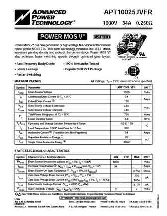
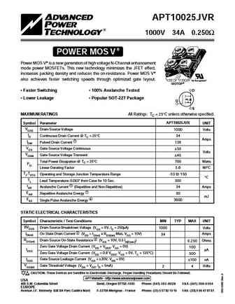
APT10025JVR 1000V 34A 0.250 POWER MOS V Power MOS V is a new generation of high voltage N-Channel enhancement mode power MOSFETs. This new technology minimizes the JFET effect, increases packing density and reduces the on-resistance. Power MOS V also achieves faster switching speeds through optimized gate layout. "UL Recognized" ISOTOP Faster Switching 100% Avalanche
apt10026l2ll.pdf
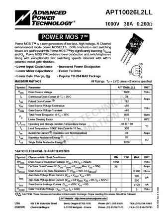
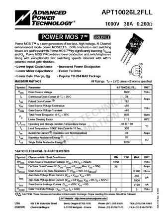
APT10026L2LL 1000V 38A 0.260W TM POWER MOS 7 Power MOS 7TM is a new generation of low loss, high voltage, N-Channel TO-264 Max enhancement mode power MOSFETS. Both conduction and switching losses are addressed with Power MOS 7TM by significantly lowering RDS(ON) and Qg. Power MOS 7TM combines lower conduction and switching losses along with exceptionally fast switching speeds inherent
apt10025jlc.pdf
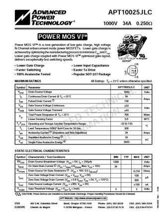
APT10025JLC 1000V 34A 0.250W TM POWER MOS VI Power MOS VITM is a new generation of low gate charge, high voltage N-Channel enhancement mode power MOSFETs. Lower gate charge is achieved by optimizing the manufacturing process to minimize Ciss and Crss. Lower gate charge coupled with Power MOS VITM optimized gate layout, "UL Recognized" delivers exceptionally fast switching speeds. ISOT
apt10025pvr.pdf
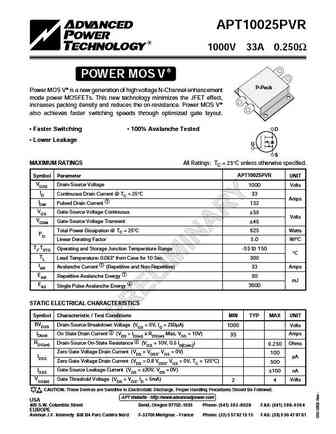
APT10025PVR 1000V 33A 0.250 POWER MOS V P-Pack Power MOS V is a new generation of high voltage N-Channel enhancement mode power MOSFETs. This new technology minimizes the JFET effect, increases packing density and reduces the on-resistance. Power MOS V also achieves faster switching speeds through optimized gate layout. Faster Switching 100% Avalanche Tested D Lowe
apt10026l2fll.pdf
APT10026L2FLL 1000V 38A 0.260W TM FREDFET POWER MOS 7 Power MOS 7TM is a new generation of low loss, high voltage, N-Channel TO-264 Max enhancement mode power MOSFETS. Both conduction and switching losses are addressed with Power MOS 7TM by significantly lowering RDS(ON) and Qg. Power MOS 7TM combines lower conduction and switching losses along with exceptionally fast switching speed
apt10026l2fllg.pdf
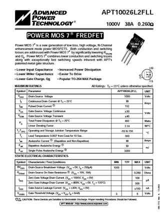
APT10026L2FLL 1000V 38A 0.260 R POWER MOS 7 FREDFET TO-264 Power MOS 7 is a new generation of low loss, high voltage, N-Channel Max enhancement mode power MOSFETS. Both conduction and switching losses are addressed with Power MOS 7 by significantly lowering RDS(ON) and Qg. Power MOS 7 combines lower conduction and switching losses along with exceptionally
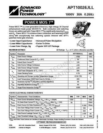
apt10026jll.pdf
APT10026JLL 1000V 30A 0.260W TM POWER MOS 7 Power MOS 7TM is a new generation of low loss, high voltage, N-Channel enhancement mode power MOSFETS. Both conduction and switching losses are addressed with Power MOS 7TM by significantly lowering RDS(ON) and Qg. Power MOS 7TM combines lower conduction and switching losses along with exceptionally fast switching speeds inherent with APT's
apt10026l2fl.pdf
APT10026L2FLL 1000V 38A 0.260W TM FREDFET POWER MOS 7 Power MOS 7TM is a new generation of low loss, high voltage, N-Channel TO-264 Max enhancement mode power MOSFETS. Both conduction and switching losses are addressed with Power MOS 7TM by significantly lowering RDS(ON) and Qg. Power MOS 7TM combines lower conduction and switching losses along with exceptionally fast switching speed
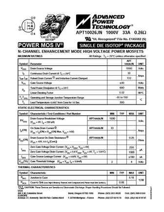
apt10026jn.pdf
D G APT10026JN 1000V 33A 0.26 S "UL Recognized" File No. E145592 (S) ISOTOP POWER MOS IV SINGLE DIE ISOTOP PACKAGE N- CHANNEL ENHANCEMENT MODE HIGH VOLTAGE POWER MOSFETS MAXIMUM RATINGS All Ratings TC = 25 C unless otherwise specified. APT Symbol Parameter 10026JN UNIT VDSS Drain-Source Voltage 1000 Volts ID Continuous Drain Current @ TC = 25 C 33 Amps IDM, lLM Pulse
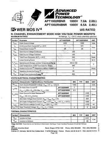
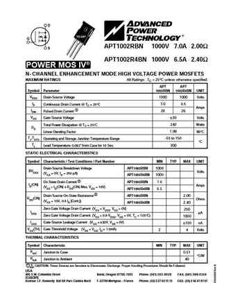
apt1002r4bn.pdf
D TO-247 G APT1002RBN 1000V 7.0A 2.00 S APT1002R4BN 1000V 6.5A 2.40 POWER MOS IV N- CHANNEL ENHANCEMENT MODE HIGH VOLTAGE POWER MOSFETS MAXIMUM RATINGS All Ratings TC = 25 C unless otherwise specified. APT APT Symbol Parameter 1002RBN 1002R4BN UNIT VDSS Drain-Source Voltage 1000 1000 Volts ID Continuous Drain Current @ TC = 25 C 7.0 6.5 Amps IDM Pulsed Drain Current 1
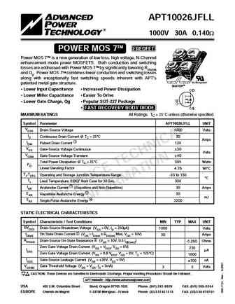
apt10026jfll.pdf
APT10026JFLL 1000V 30A 0.140W TM FREDFET POWER MOS 7 Power MOS 7TM is a new generation of low loss, high voltage, N-Channel enhancement mode power MOSFETS. Both conduction and switching losses are addressed with Power MOS 7TM by significantly lowering RDS(ON) and Qg. Power MOS 7TM combines lower conduction and switching losses along with exceptionally fast switching speeds inherent wi
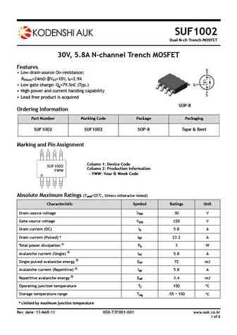
suf1002.pdf
SUF1002 Dual N-ch Trench MOSFET 30V, 5.8A N-channel Trench MOSFET Features Low drain-source On-resistance RDS(on)=24m @VGS=10V, ID=2.9A Low gate charge Qg=79.5nC (Typ.) High power and current handing capability Lead free product is acquired SOP-8 Ordering Information Part Number Marking Code Package Packaging SUF1002 SUF1002 SOP-8 Tape & Reel Marki
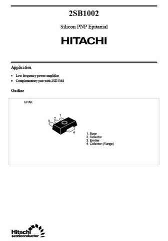
2sb1002.pdf
2SB1002 Silicon PNP Epitaxial Application Low frequency power amplifier Complementary pair with 2SD1368 Outline UPAK 1 2 3 4 1. Base 2. Collector 3. Emitter 4. Collector (Flange) 2SB1002 Absolute Maximum Ratings (Ta = 25 C) Item Symbol Ratings Unit Collector to base voltage VCBO 70 V Collector to emitter voltage VCEO 50 V Emitter to base voltage VEBO 6 V
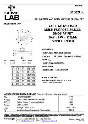
d1002uk.pdf
TetraFET D1002UK ROHS COMPLIANT METAL GATE RF SILICON FET MECHANICAL DATA GOLD METALLISED A MULTI-PURPOSE SILICON B C DMOS RF FET 1 2 40W 28V 175MHz D 4 3 E SINGLE ENDED M F G FEATURES SIMPLIFIED AMPLIFIER DESIGN H K I J SUITABLE FOR BROAD BAND APPLICATIONS DA LOW Crss PIN 1 SOURCE PIN 2 DRAIN PIN 3 SOURCE PIN 4 GATE SIMPLE BIAS CIRCUITS
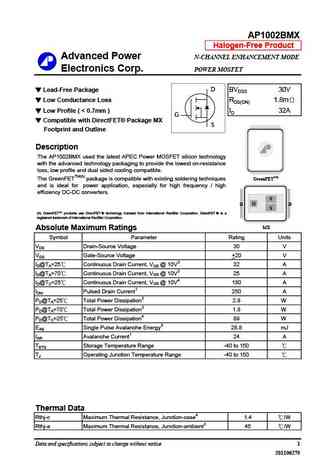
ap1002bmx.pdf
AP1002BMX Halogen-Free Product Advanced Power N-CHANNEL ENHANCEMENT MODE Electronics Corp. POWER MOSFET Lead-Free Package D BVDSS 30V Low Conductance Loss RDS(ON) 1.8m Low Profile (
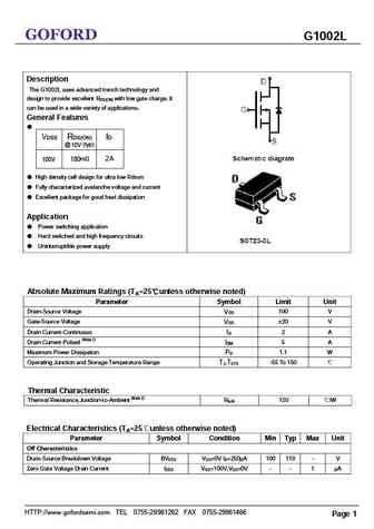
g1002l.pdf
GOFORD G1002L Description The G1002L uses advanced trench technology and design to provide excellent RDS(ON) with low gate charge. It can be used in a wide variety of applications. General Features VDSS RDS(ON) ID @ 10V (typ) 2A m 100V 180 High density cell design for ultra low Rdson Fully characterized avalanche voltage and current Excellent package f
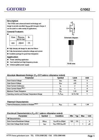
g1002 to92.pdf
GOFORD G1002 Description D The G1002 uses advanced trench technology and design to provide excellent RDS(ON) with low gate charge. It G can be used in a wide variety of applications. General Features S VDSS RDS(ON) ID Schematic diagram @ 10V (typ) 2A m 100V 200 High density cell design for ultra low Rdson Fully characterized avalanche voltage and curren
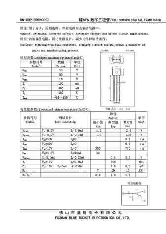
rn1002.pdf
RN1002(3RC1002) NPN /SILICON NPN DIGITAL TRANSISTOR Purpose Switching, inverter circuit, interface circuit and driver circuit applications. Features With built-in bias resistors, simplify circuit design, reduce a q
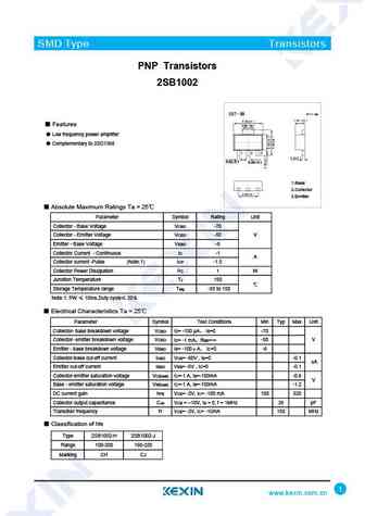
2sb1002.pdf
SMD Type Transistors PNP Transistors 2SB1002 Features 1.70 0.1 Low frequency power amplifier Complementary to 2SD1368 0.42 0.1 0.46 0.1 1.Base 2.Collector 3.Emitter Absolute Maximum Ratings Ta = 25 Parameter Symbol Rating Unit Collector - Base Voltage VCBO -70 Collector - Emitter Voltage VCEO -50 V Emitter - Base Voltage VEBO -6 Collector Current - Cont
mrf1002ma.pdf
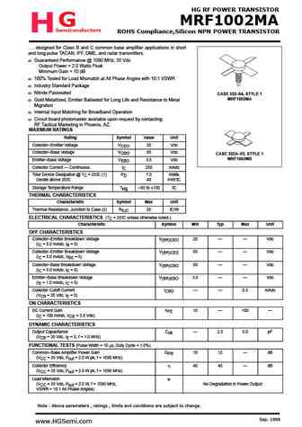
HG RF POWER TRANSISTOR MRF1002MA Semiconductors HG ROHS Compliance,Silicon NPN POWER TRANSISTOR . . . designed for Class B and C common base amplifier applications in short and long pulse TACAN, IFF, DME, and radar transmitters. Guaranteed Performance @ 1090 MHz, 35 Vdc Output Power = 2.0 Watts Peak Minimum Gain = 10 dB 100% Tested for Load Mismatch at All Phase Angles with 10 1
mrf1002mb.pdf
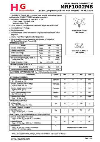
HG RF POWER TRANSISTOR MRF1002MB Semiconductors HG ROHS Compliance,Silicon NPN POWER TRANSISTOR . . . designed for Class B and C common base amplifier applications in short and long pulse TACAN, IFF, DME, and radar transmitters. Guaranteed Performance @ 1090 MHz, 35 Vdc Output Power = 2.0 Watts Peak Minimum Gain = 10 dB 100% Tested for Load Mismatch at All Phase Angles with 10 1
sef401002.pdf
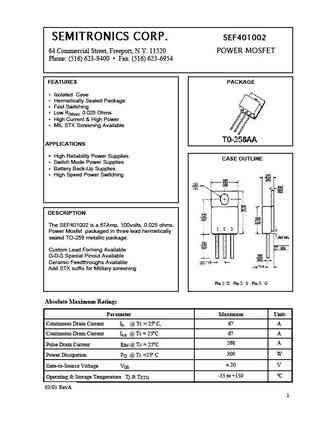
SEMITRONICS CORP. SEF401002 64 Commercial Street, Freeport, N.Y. 11520 POWER MOSFET Phone (516) 623-9400 Fax. (516) 623-6954 FEATURES PACKAGE Isolated Case Hermetically Sealed Package Fast Switching Low RDS(on) 0.025 Ohms High Current & High Power MIL STX Screening Available APPLICATIONS High Reliability Power Supplies CASE OUT
spm1002.pdf
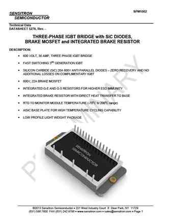
SPM1002 SENSITRON SEMICONDUCTOR Technical Data DATASHEET 5278, Rev. - THREE-PHASE IGBT BRIDGE with SiC DIODES, BRAKE MOSFET and INTEGRATED BRAKE RESISTOR DESCRIPTION 600 VOLT, 30 AMP, THREE PHASE IGBT BRIDGE FAST SWITCHING 3RD GENERATION IGBT SILICON CARBIDE (SiC) 20A 600V ANTI PARALLEL DIODES ZERO RECOVERY AND NO ADDITIONAL LOSSES ON COMPLIMENTARY IGBT
sradm1002.pdf
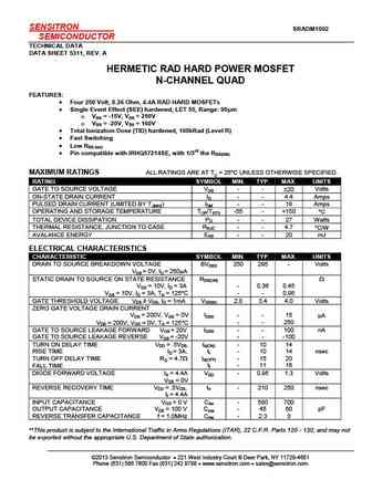
SENSITRON SRADM1002 SEMICONDUCTOR TECHNICAL DATA DATA SHEET 5311, REV. A HERMETIC RAD HARD POWER MOSFET N-CHANNEL QUAD FEATURES Four 250 Volt, 0.36 Ohm, 4.4A RAD HARD MOSFETs Single Event Effect (SEE) hardened, LET 55, Range 90 m o VGS = -15V, VDS = 250V o VGS = -20V, VDS = 160V Total Ionization Dose (TID) hardened, 100kRad (Level R) Fast Switching
sl1002b.pdf
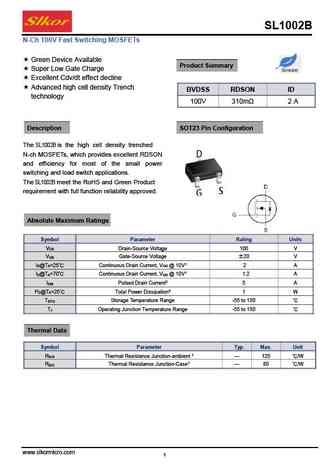
SL1002B N-Ch 100V Fast Switching MOSFETs Green Device Available Product Summary Super Low Gate Charge Excellent Cdv/dt effect decline Advanced high cell density Trench BVDSS RDSON ID technology 100V 310m 2 A Description SOT23 Pin Configuration The SL1002B is the high cell density trenched N-ch MOSFETs, which provides excellent RDSON and efficiency for m
st1002.pdf
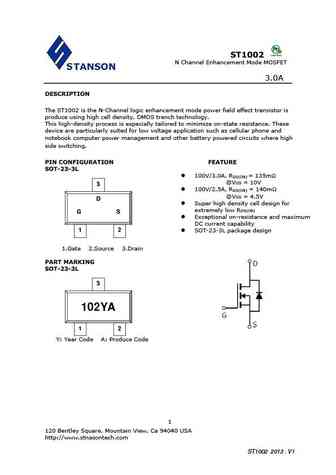
ST1002 N Channel Enhancement Mode MOSFET 3.0A DESCRIPTION The ST1002 is the N-Channel logic enhancement mode power field effect transistor is produce using high cell density, DMOS trench technology. This high-density process is especially tailored to minimize on-state resistance. These device are particularly suited for low voltage application such as cellular phone and notebo
jmsh1002ytl.pdf
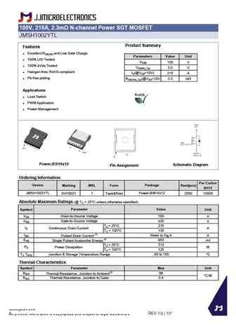
100V, 215A, 2.3m N-channel Power SGT MOSFET JMSH1002YTL Product Summary Features Excellent RDS(ON) and Low Gate Charge Parameters Value Unit 100% UIS Tested VDSS 100 V 100% Vds Tested VGS(th)_Typ 3.0 V Halogen-free; RoHS-compliant ID(@VGS=10V) 215 A Pb-free plating RDS(ON)_Typ(@VGS=10V 2.3 mW Applications Load Switch PWM Application Power Ma
jmsh1002aeq.pdf
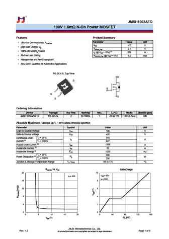
JMSH1002AEQ 100V 1.6m N-Ch Power MOSFET Features Product Summary Parameter Value Unit Ultra-low ON-resistance, RDS(ON) VDS 100 V Low Gate Charge, Qg VGS(th)_Typ 2.7 V 100% UIS and Rg Tested ID (@ VGS = 10V) (1) 350 A Pb-free Lead Plating RDS(ON)_Typ (@ VGS = 10V) 1.6 m Halogen-free and RoHS-compliant AEC-Q101 Qualified for Automotive Applications
jmsh1002tc jmsh1002te.pdf
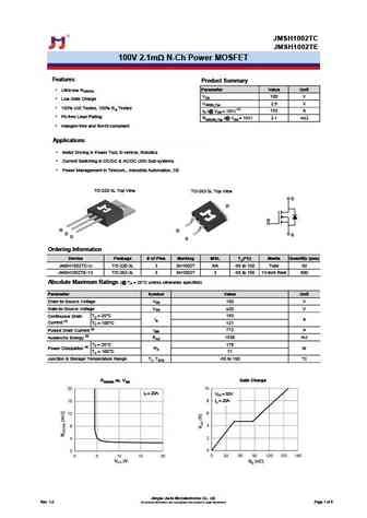
JMSH1002TC JMSH1002TE 100V 2.1mW N-Ch Power MOSFET Features Product Summary Parameter Value Unit Ultra-low RDS(ON) Ultra-low RDS(ON) VDS 100 V Low Gate Charge Low Gate Charge VGS(th)_Typ 2.9 V 100% UIS Tested, 100% R 100% UIS Tested, 100% Rgg Tested Tested ID (@ VGS = 10V) (1) 193 A Pb-free Lead Plating Pb-free Lead Plating RDS(ON)_Typ (@ VGS
jmsh1002nc jmsh1002ne.pdf
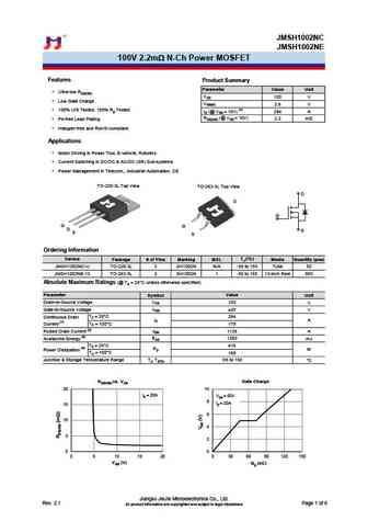
JMSH1002NC JMSH1002NE 100V 2.2m N-Ch Power MOSFET Features Product Summary Parameter Value Unit Ultra-low RDS(ON) VDS 100 V Low Gate Charge VGS(th) 2.8 V 100% UIS Tested, 100% Rg Tested ID (@ VGS = 10V) (1) 284 A RDS(ON) (@ VGS = 10V) 2.2 m Pb-free Lead Plating Halogen-free and RoHS-compliant Applications Motor Driving in Power Tool, E-vehicl
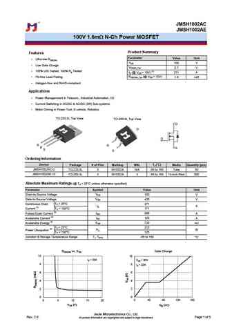
jmsh1002ac jmsh1002ae.pdf
JMSH1002AC JMSH1002AE 100V 1.6mW N-Ch Power MOSFET Product Summary Features Parameter Value Unit Ultra-low RDS(ON) VDS 100 V Low Gate Charge VGS(th)_Typ 2.7 V 100% UIS Tested, 100% Rg Tested ID (@ VGS = 10V) (1) 271 A RDS(ON)_Typ (@ VGS = 10V) Pb-free Lead Plating 1.6 mW Halogen-free and RoHS-compliant Applications Power Managerment in Telecom., Ind
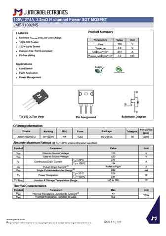
jmsh1002ns.pdf
100V, 274A, 3.2m N-channel Power SGT MOSFET JMSH1002NS Product Summary Features Excellent RDS(ON) and Low Gate Charge Parameters Value Unit 100% UIS Tested VDSS 100 V 100% Vds Tested VGS(th)_Typ 2.8 V Halogen-free; RoHS-compliant ID(@VGS=10V) 274 A Pb-free plating RDS(ON)_Typ(@VGS=10V 3.2 mW Applications Load Switch PWM Application Power Man
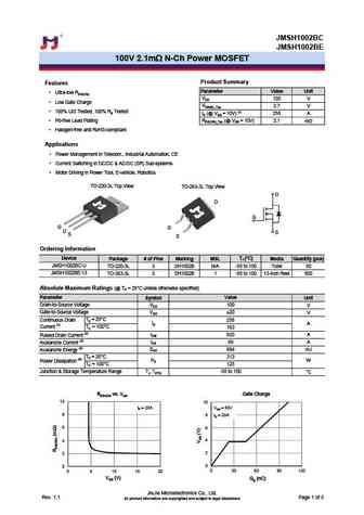
jmsh1002bc jmsh1002be.pdf
JMSH1002BC JMSH1002BE 100V 2.1m N-Ch Power MOSFET Product Summary Features Parameter Value Unit Ultra-low RDS(ON) VDS 100 V Low Gate Charge VGS(th)_Typ 2.7 V 100% UIS Tested, 100% Rg Tested ID (@ VGS = 10V) (1) 258 A Pb-free Lead Plating RDS(ON)_Typ (@ VGS = 10V) 2.1 m Halogen-free and RoHS-compliant Applications Power Management in Telecom., I
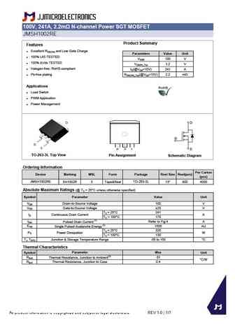
jmsh1002re.pdf
100V, 241A, 2.2m N-channel Power SGT MOSFET JMSH1002RE Product Summary Features Excellent RDS(ON) and Low Gate Charge Parameters Value Unit 100% UIS TESTED VDSS 100 V 100% Vds TESTED VGS(th)_Typ 3.2 V Halogen-free; RoHS-compliant ID(@VGS=10V) 241 A Pb-free plating RDS(ON)_Typ(@VGS=10V) 2.2 mW Applications Load Switch PWM Application Power Mana
jmsh1002as.pdf
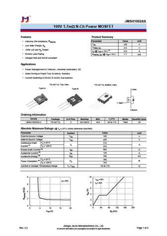
JMSH1002AS 100V 1.7mW N-Ch Power MOSFET Features Product Summary Parameter Value Unit Ultra-low ON-resistance, RDS(ON) VDS 100 V Low Gate Charge, Qg VGS(th)_Typ 2.8 V 100% UIS and Rg Tested ID (@ VGS = 10V) (1) 314 A Pb-free Lead Plating RDS(ON)_Typ (@ VGS = 10V) 1.7 mW Halogen-free and RoHS-compliant Applications Power Managerment in Telecom., Indus
jmsh1002asq.pdf
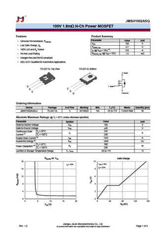
JMSH1002ASQ 100V 1.8m N-Ch Power MOSFET Features Product Summary Parameter Value Unit Ultra-low ON-resistance, RDS(ON) VDS 100 V Low Gate Charge, Qg VGS(th)_Typ 2.7 V 100% UIS and Rg Tested ID (@ VGS = 10V) (1) 333 A RDS(ON)_Typ (@ VGS = 10V) 1.8 Pb-free Lead Plating m Halogen-free and RoHS-compliant AEC-Q101 Qualified for Automotive Application
jmsh1002yc jmsh1002ye.pdf
JMSH1002YC JMSH1002YE 100V 3.1mW N-Ch Power MOSFET Features Product Summary Parameter Value Unit Ultra-low RDS(ON) Ultra-low RDS(ON) VDS 100 V Low Gate Charge Low Gate Charge VGS(th)_Typ 3.2 V 100% UIS Tested, 100% R 100% UIS Tested, 100% Rgg Tested Tested ID (@ VGS = 10V) (1) 175 A Pb-free Lead Plating Pb-free Lead Plating RDS(ON)_Typ (@ VGS
jmsh1002ttl.pdf
100V, 280A, 1.6m N-channel Power SGT MOSFET JMSH1002TTL Product Summary Features Excellent RDS(ON) and Low Gate Charge Parameters Value Unit 100% UIS Tested VDSS 100 V 100% Vds Tested VGS(th)_Typ 3.0 V Halogen-free; RoHS-compliant ID(@VGS=10V) 280 A RDS(ON)_Typ(@VGS=10V 1.6 mW Applications Load Switch PWM Application Power Management PowerJE 10
jmsh1002ntl.pdf
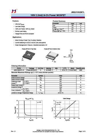
JMSH1002NTL 100V 2.0m N-Ch Power MOSFET Features Product Summary Parameter Value Unit Ultra-low RDS(ON) VDS 100 V Low Gate Charge VGS(th) 3.0 V 100% UIS Tested, 100% Rg Tested ID (@ VGS = 10V) (1) 337 A RDS(ON) (@ VGS = 10V) 2.0 m Pb-free Lead Plating Halogen-free and RoHS-compliant Applications Motor Driving in Power Tool, E-vehicle, Robotics
se100250gts.pdf
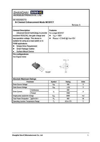
SE100250GTS N-Channel Enhancement-Mode MOSFET Revision A General Description Features For a single MOSFET Advanced trench technology to provide excellent RDS(ON), low gate charge and V = 100V DS low operation voltage. This device is R =2.5m @V =10V DS(ON) GS suitable for using as a load switch or in PWM applications. Simple Drive Requirement Small Package Outlin
2sa1002.pdf
isc Silicon PNP Power Transistor 2SA1002 DESCRIPTION High Current Capability Collector-Emitter Breakdown Voltage- V = -120V(Min.) (BR)CEO Minimum Lot-to-Lot variations for robust device performance and reliable operation APPLICATIONS Designed for audio and general purpose applications. ABSOLUTE MAXIMUM RATINGS(T =25 ) a SYMBOL PARAMETER VALUE UNIT V Collector-Base Volta
Otros transistores... 90N03 , SSS10N60 , SSS12N60 , SSS1N60 , SSS2N60 , SSS5N60 , SSS7N60 , SSS8N60 , IRFB7545 , 1115 , 1515 , G1601 , 2300 , 2301 , 2302 , 3035 , 3400 .
🌐 : EN ES РУ
Liste
Recientemente añadidas las descripciónes de los transistores:
MOSFET: ASD80R750E | ASD70R950E | ASD70R600E | ASD70R380E | ASD65R850E | ASD65R550E | ASD65R350E | ASD65R300E | ASD65R280E | ASD65R270E | ASD60R330E | ASD60R280E | ASB80R750E | ASB70R380E | ASB65R300E | ASB65R220E
Popular searches
pk6d0ba mosfet | 2sd726 | c536 transistor equivalent | 2sa1294 datasheet | mp10b transistor | bc182b | 2n3054 transistor equivalent | 2n554
