FTK4822 MOSFET Equivalente. Reemplazo. Hoja de especificaciones. Principales características
Número de Parte: FTK4822
Tipo de FET: MOSFET
Polaridad de transistor: N
ESPECIFICACIONES MÁXIMAS
Pdⓘ - Máxima disipación de potencia: 1.4 W
|Vds|ⓘ - Voltaje máximo drenador-fuente: 30 V
|Vgs|ⓘ - Voltaje máximo fuente-puerta: 20 V
|Id|ⓘ - Corriente continua de drenaje: 8.5 A
Tjⓘ - Temperatura máxima de unión: 150 °C
CARACTERÍSTICAS ELÉCTRICAS
trⓘ - Tiempo de subida: 6.5 nS
Cossⓘ - Capacitancia de salida: 180 pF
RDSonⓘ - Resistencia estado encendido drenaje a fuente: 0.016 Ohm
Encapsulados: SOP8
Búsqueda de reemplazo de FTK4822 MOSFET
- Selecciónⓘ de transistores por parámetros
FTK4822 datasheet
ftk4822.pdf
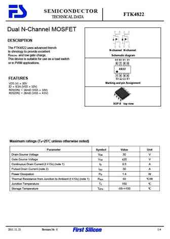
SEMICONDUCTOR FTK4822 TECHNICAL DATA Dual N-Channel MOSFET DESCRIPTION The FTK4822 uses advanced trench N-channel N-channel te chnology to provide excellent RDS(ON) and low gate charge. Schematic diagram This device is suitable for use as a load switch D 2 D 2 D 1 D 1 or in PWM applications. 6 5 8 7 4822 1 2 4 3 FEATURES S 2 G 2 G 1 S 1 Marking and pin Assignment VD
ftk4828f.pdf
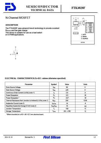
SEMICONDUCTOR FTK4828F TECHNICAL DATA A C N-Channel MOSFET H G DIM MILLIMETERS A 4.70 MAX _ B 2.50 0.20 DESCRIPTION C 1.70 MAX D D D 0.45 0.15/-0.10 K E 4.25 MAX _ The FTK4828F uses advancd trench technology to provide excellent F F F 1.50 0.10 G 0.40 TYP H 1.7 MAX RDS(ON) and low gate charge. J 0.7 MIN K 0.5 0.15/-0.10 1 2 3 This device is suitable for use as a lo
ftk4828d.pdf
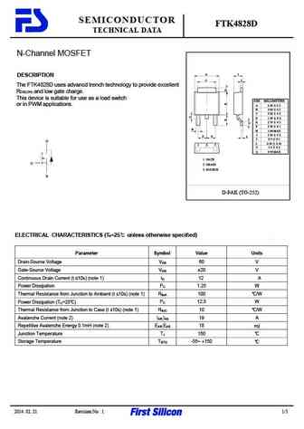
SEMICONDUCTOR FTK4828D TECHNICAL DATA N-Channel MOSFET A I DESCRIPTION C J The FTK4828D uses advancd trench technology to provide excellent RDS(ON) and low gate charge. This device is suitable for use as a load switch DIM MILLIMETERS or in PWM applications. A 6 50 0 2 B 5 60 0 2 C 5 20 0 2 D 1 50 0 2 E 2 70 0 2 F 2 30 0 1 H H 1 00 MAX I 2 30 0 2
ftk4828.pdf
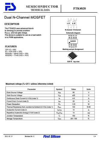
SEMICONDUCTOR FTK4828 TECHNICAL DATA Dual N-Channel MOSFET DESCRIPTION The FTK4828 uses advanced trench N-channel N-channel te chnology to provide excellent RDS(ON) and low gate charge. Schematic diagram This device is suitable for use as a load switch D 2 D 2 D 1 D 1 or in PWM applications. 6 5 8 7 Q4828 1 2 4 3 FEATURES S 2 G 2 G 1 S 1 Marking and pin Assignment V
Otros transistores... FTK4410D, FTK4414, FTK4435, FTK4438, FTK4459, FTK4503, FTK4604, FTK4703, K3569, FTK4828, FTK4828D, FTK4828F, FTK4953, 2SJ463A, 2SK1723, 2SK2769-01MR, 2SK3113
🌐 : EN ES РУ

Liste
Recientemente añadidas las descripciónes de los transistores:
MOSFET: AUW033N08BG | AUW025N10 | AUR030N10 | AUR020N10 | AUR020N085 | AUR014N10 | AUP074N10 | AUP065N10 | AUP062N08BG | AUP060N08AG | HYG053N10NS1B | HYG053N10NS1P | AP220N04T | AP220N04P | QM3126M3 | AUP060N055
Popular searches
bc546 datasheet | mpsa06 transistor | tta004b | 2sc1116 | 2n3565 equivalent | 10n60 | 2sc1061 | a1023