FTK4822 Specs and Replacement
Type Designator: FTK4822
Type of Transistor: MOSFET
Type of Control Channel: N-Channel
Absolute Maximum Ratings
Pd ⓘ - Maximum Power Dissipation: 1.4 W
|Vds|ⓘ - Maximum Drain-Source Voltage: 30 V
|Vgs|ⓘ - Maximum Gate-Source Voltage: 20 V
|Id| ⓘ - Maximum Drain Current: 8.5 A
Tj ⓘ - Maximum Junction Temperature: 150 °C
Electrical Characteristics
tr ⓘ - Rise Time: 6.5 nS
Cossⓘ - Output Capacitance: 180 pF
RDSonⓘ - Maximum Drain-Source On-State Resistance: 0.016 Ohm
Package: SOP8
FTK4822 substitution
- MOSFET ⓘ Cross-Reference Search
FTK4822 datasheet
ftk4822.pdf
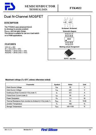
SEMICONDUCTOR FTK4822 TECHNICAL DATA Dual N-Channel MOSFET DESCRIPTION The FTK4822 uses advanced trench N-channel N-channel te chnology to provide excellent RDS(ON) and low gate charge. Schematic diagram This device is suitable for use as a load switch D 2 D 2 D 1 D 1 or in PWM applications. 6 5 8 7 4822 1 2 4 3 FEATURES S 2 G 2 G 1 S 1 Marking and pin Assignment VD... See More ⇒
ftk4828f.pdf
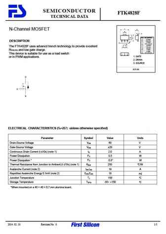
SEMICONDUCTOR FTK4828F TECHNICAL DATA A C N-Channel MOSFET H G DIM MILLIMETERS A 4.70 MAX _ B 2.50 0.20 DESCRIPTION C 1.70 MAX D D D 0.45 0.15/-0.10 K E 4.25 MAX _ The FTK4828F uses advancd trench technology to provide excellent F F F 1.50 0.10 G 0.40 TYP H 1.7 MAX RDS(ON) and low gate charge. J 0.7 MIN K 0.5 0.15/-0.10 1 2 3 This device is suitable for use as a lo... See More ⇒
ftk4828d.pdf
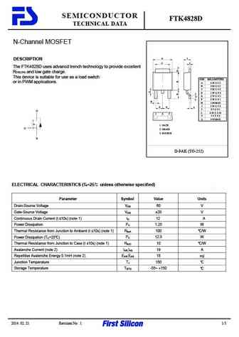
SEMICONDUCTOR FTK4828D TECHNICAL DATA N-Channel MOSFET A I DESCRIPTION C J The FTK4828D uses advancd trench technology to provide excellent RDS(ON) and low gate charge. This device is suitable for use as a load switch DIM MILLIMETERS or in PWM applications. A 6 50 0 2 B 5 60 0 2 C 5 20 0 2 D 1 50 0 2 E 2 70 0 2 F 2 30 0 1 H H 1 00 MAX I 2 30 0 2... See More ⇒
ftk4828.pdf
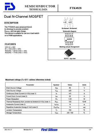
SEMICONDUCTOR FTK4828 TECHNICAL DATA Dual N-Channel MOSFET DESCRIPTION The FTK4828 uses advanced trench N-channel N-channel te chnology to provide excellent RDS(ON) and low gate charge. Schematic diagram This device is suitable for use as a load switch D 2 D 2 D 1 D 1 or in PWM applications. 6 5 8 7 Q4828 1 2 4 3 FEATURES S 2 G 2 G 1 S 1 Marking and pin Assignment V... See More ⇒
Detailed specifications: FTK4410D, FTK4414, FTK4435, FTK4438, FTK4459, FTK4503, FTK4604, FTK4703, K3569, FTK4828, FTK4828D, FTK4828F, FTK4953, 2SJ463A, 2SK1723, 2SK2769-01MR, 2SK3113
Keywords - FTK4822 MOSFET specs
FTK4822 cross reference
FTK4822 equivalent finder
FTK4822 pdf lookup
FTK4822 substitution
FTK4822 replacement
Need a MOSFET replacement? Our guide shows you how to find a perfect substitute by comparing key parameters and specs
🌐 : EN ES РУ

LIST
Last Update
MOSFET: AUW033N08BG | AUW025N10 | AUR030N10 | AUR020N10 | AUR020N085 | AUR014N10 | AUP074N10 | AUP065N10 | AUP062N08BG | AUP060N08AG
Popular searches
bc546 datasheet | mpsa06 transistor | tta004b | 2sc1116 | 2n3565 equivalent | 10n60 | 2sc1061 | a1023