17N60 MOSFET Equivalente. Reemplazo. Hoja de especificaciones. Principales características
Número de Parte: 17N60
Tipo de FET: MOSFET
Polaridad de transistor: N
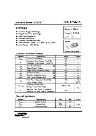
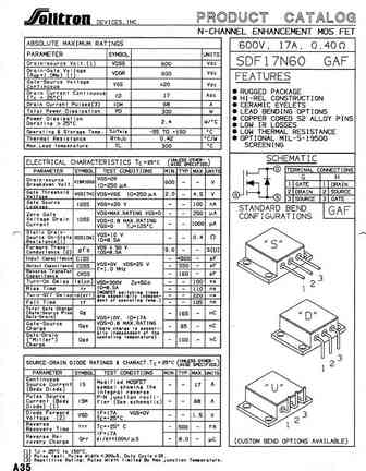
ESPECIFICACIONES MÁXIMAS
Pdⓘ - Máxima disipación de potencia: 250 W
|Vds|ⓘ - Voltaje máximo drenador-fuente: 600 V
|Vgs|ⓘ - Voltaje máximo fuente-puerta: 30 V
|Id|ⓘ - Corriente continua de drenaje: 17 A
Tjⓘ - Temperatura máxima de unión: 150 °C
CARACTERÍSTICAS ELÉCTRICAS
trⓘ - Tiempo de subida: 110 nS
Cossⓘ - Capacitancia de salida: 140 pF
RDSonⓘ - Resistencia estado encendido drenaje a fuente: 0.45 Ohm
Encapsulados: TO-3
Búsqueda de reemplazo de 17N60 MOSFET
- Selecciónⓘ de transistores por parámetros
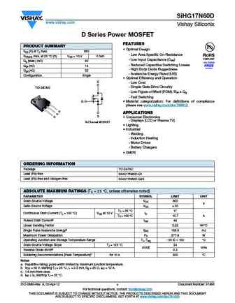
17N60 datasheet
17n60.pdf
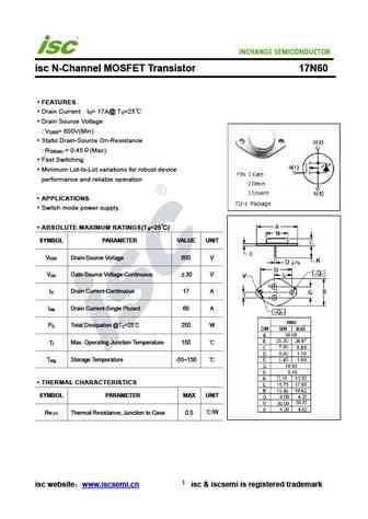
isc N-Channel MOSFET Transistor 17N60 FEATURES Drain Current I = 17A@ T =25 D C Drain Source Voltage V = 600V(Min) DSS Static Drain-Source On-Resistance R = 0.45 (Max) DS(on) Fast Switching Minimum Lot-to-Lot variations for robust device performance and reliable operation APPLICATIONS Switch mode power supply. ABSOLUTE MAXIMUM RATINGS(T =25 ) a SYMBO
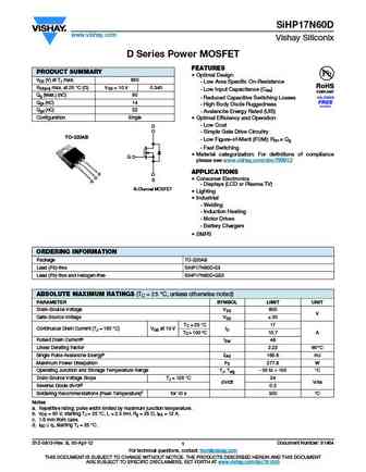
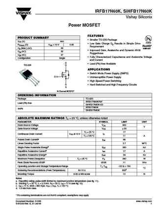
irfb17n60k.pdf
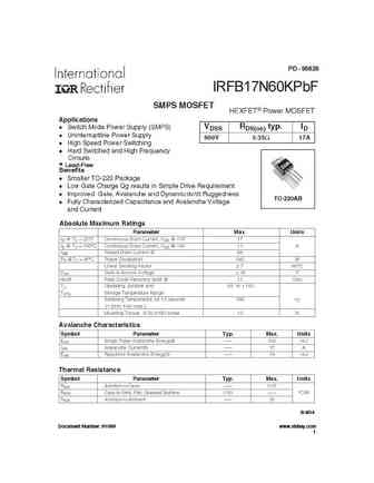
PD - 95629 IRFB17N60KPbF Lead-Free 8/4/04 Document Number 91099 www.vishay.com 1 IRFB17N60KPbF Document Number 91099 www.vishay.com 2 IRFB17N60KPbF Document Number 91099 www.vishay.com 3 IRFB17N60KPbF Document Number 91099 www.vishay.com 4 IRFB17N60KPbF Document Number 91099 www.vishay.com 5 IRFB17N60KPbF Document Number 91099 www.vishay.com 6 IRFB17N60KPbF
fdp17n60n fdpf17n60nt.pdf
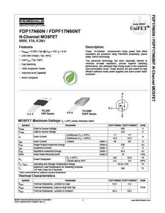
July 2009 UniFETTM FDP17N60N / FDPF17N60NT N-Channel MOSFET 600V, 17A, 0.34 Features Description RDS(on) = 0.29 ( Typ.)@ VGS = 10V, ID = 8.5A These N-Channel enhancement mode power field effect transistors are produced using Fairchild s proprietary, planar Low Gate Charge ( Typ. 48nC) stripe, DMOS technology. Low Crss ( Typ. 23pF) This advanced technology has b

Otros transistores... 10N45 , 12N18 , 12N20 , 12N45 , 12N45A , 15N05 , 15N12 , 15N45 , IRFP250 , 2SJ374 , 2SK1009 , 2SK1010 , 2SK1011 , 2SK1012 , 2SK1013 , 2SK1014 , 2SK1023 .
History: G1NP02ELL | SID9971 | AP3N2R8H | SES760 | HY1001P | BUK457-400A | 2SJ0582
History: G1NP02ELL | SID9971 | AP3N2R8H | SES760 | HY1001P | BUK457-400A | 2SJ0582
🌐 : EN ES РУ

Liste
Recientemente añadidas las descripciónes de los transistores:
MOSFET: AUB062N08BG | AUB060N08AG | AUB056N10 | AUB056N08BGL | AUB050N085 | AUB050N055 | AUB045N12 | AUB045N10BT | AUB039N10 | AUB034N10 | AUB033N08BG | AUB026N085 | AUA062N08BG | AUA060N08AG | AUA056N08BGL | AUA039N10
Popular searches
tip141 | 2n404 | 2n4250 | d882 transistor equivalent | 17n80c3 | bc107 transistor | rjp63g4 datasheet | 2sc1115