17N60 Specs and Replacement
Type Designator: 17N60
Type of Transistor: MOSFET
Type of Control Channel: N-Channel
Absolute Maximum Ratings
Pd ⓘ
- Maximum Power Dissipation: 250 W
|Vds|ⓘ - Maximum Drain-Source Voltage: 600 V
|Vgs|ⓘ - Maximum Gate-Source Voltage: 30 V
|Id| ⓘ - Maximum Drain Current: 17 A
Tj ⓘ - Maximum Junction Temperature: 150 °C
Electrical Characteristics
tr ⓘ - Rise Time: 110 nS
Cossⓘ -
Output Capacitance: 140 pF
RDSonⓘ - Maximum Drain-Source On-State Resistance: 0.45 Ohm
Package: TO-3
- MOSFET ⓘ Cross-Reference Search
17N60 datasheet
..1. Size:211K inchange semiconductor
17n60.pdf 
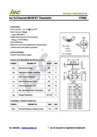
isc N-Channel MOSFET Transistor 17N60 FEATURES Drain Current I = 17A@ T =25 D C Drain Source Voltage V = 600V(Min) DSS Static Drain-Source On-Resistance R = 0.45 (Max) DS(on) Fast Switching Minimum Lot-to-Lot variations for robust device performance and reliable operation APPLICATIONS Switch mode power supply. ABSOLUTE MAXIMUM RATINGS(T =25 ) a SYMBO... See More ⇒
0.2. Size:486K international rectifier
irfb17n60k.pdf
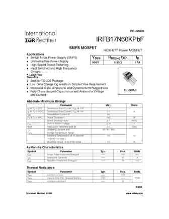
PD - 95629 IRFB17N60KPbF Lead-Free 8/4/04 Document Number 91099 www.vishay.com 1 IRFB17N60KPbF Document Number 91099 www.vishay.com 2 IRFB17N60KPbF Document Number 91099 www.vishay.com 3 IRFB17N60KPbF Document Number 91099 www.vishay.com 4 IRFB17N60KPbF Document Number 91099 www.vishay.com 5 IRFB17N60KPbF Document Number 91099 www.vishay.com 6 IRFB17N60KPbF ... See More ⇒
0.3. Size:761K fairchild semi
fdp17n60n fdpf17n60nt.pdf
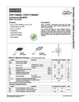
July 2009 UniFETTM FDP17N60N / FDPF17N60NT N-Channel MOSFET 600V, 17A, 0.34 Features Description RDS(on) = 0.29 ( Typ.)@ VGS = 10V, ID = 8.5A These N-Channel enhancement mode power field effect transistors are produced using Fairchild s proprietary, planar Low Gate Charge ( Typ. 48nC) stripe, DMOS technology. Low Crss ( Typ. 23pF) This advanced technology has b... See More ⇒
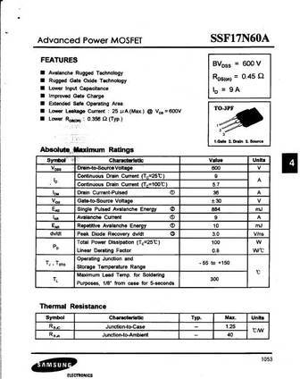
0.4. Size:944K samsung
ssh17n60a.pdf
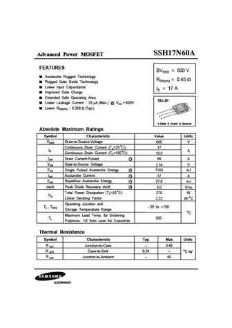
Advanced Power MOSFET FEATURES BVDSS = 600 V Avalanche Rugged Technology RDS(on) = 0.45 Rugged Gate Oxide Technology Lower Input Capacitance ID = 17 A Improved Gate Charge Extended Safe Operating Area Lower Leakage Current 25 A (Max.) @ VDS = 600V Lower RDS(ON) 0.356 (Typ.) 1 2 3 1.Gate 2. Drain 3. Source Absolute Maximum Ratings Symbol Characteristic Va... See More ⇒
0.5. Size:219K vishay
sihp17n60d.pdf
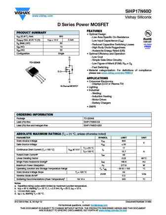
SiHP17N60D www.vishay.com Vishay Siliconix D Series Power MOSFET FEATURES PRODUCT SUMMARY Optimal Design VDS (V) at TJ max. 650 - Low Area Specific On-Resistance RDS(on) max. at 25 C ( ) VGS = 10 V 0.340 - Low Input Capacitance (Ciss) Qg (Max.) (nC) 90 - Reduced Capacitive Switching Losses Qgs (nC) 14 - High Body Diode Ruggedness Qgd (nC) 22 - Avalanche Energy Rated (UIS... See More ⇒
0.6. Size:187K vishay
sihg17n60d.pdf
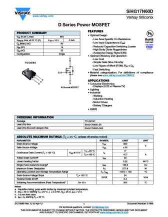
SiHG17N60D www.vishay.com Vishay Siliconix D Series Power MOSFET FEATURES PRODUCT SUMMARY Optimal Design VDS (V) at TJ max. 650 - Low Area Specific On-Resistance RDS(on) max. at 25 C ( ) VGS = 10 V 0.340 - Low Input Capacitance (Ciss) Qg (Max.) (nC) 90 - Reduced Capacitive Switching Losses Qgs (nC) 14 - High Body Diode Ruggedness Qgd (nC) 22 - Avalanche Energy Rated (UIS... See More ⇒
0.7. Size:1018K vishay
irfb17n60k irfb17n60kpbf.pdf
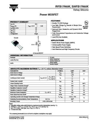
IRFB17N60K, SiHFB17N60K Vishay Siliconix Power MOSFET FEATURES PRODUCT SUMMARY Smaller TO-220 Package VDS (V) 600 Available Low Gate Charge Qg Results in Simple Drive RDS(on) ( )VGS = 10 V 0.35 RoHS* Requirement Qg (Max.) (nC) 99 COMPLIANT Improved Gate, Avalanche and Dynamic dV/dt Qgs (nC) 32 Ruggedness Qgd (nC) 47 Fully Characterized Capacitance and Avalanc... See More ⇒
0.8. Size:525K fuji
fmh17n60es.pdf
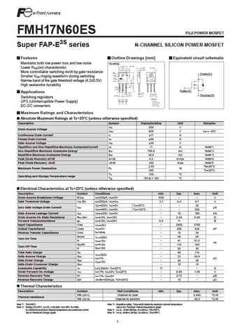
FMH17N60ES FUJI POWER MOSFET Super FAP-E3S series N-CHANNEL SILICON POWER MOSFET Features Outline Drawings [mm] Equivalent circuit schematic Maintains both low power loss and low noise TO-3P(Q) Lower R (on) characteristic DS More controllable switching dv/dt by gate resistance Drain(D) Smaller V ringing waveform during switching GS Narrow band of the gate threshold voltage (4.2 0.5V... See More ⇒
0.9. Size:517K fuji
fmr17n60es.pdf

FMR17N60ES FUJI POWER MOSFET Super FAP-E3S series N-CHANNEL SILICON POWER MOSFET Features Outline Drawings [mm] Equivalent circuit schematic Maintains both low power loss and low noise TO-3PF Lower R (on) characteristic DS More controllable switching dv/dt by gate resistance Drain(D) Smaller V ringing waveform during switching GS Narrow band of the gate threshold voltage (4.2 0.5V) ... See More ⇒
0.10. Size:514K fuji
fmv17n60es.pdf
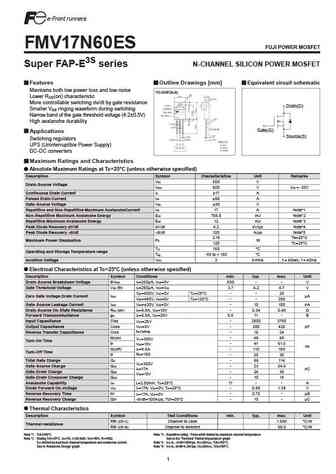
FMV17N60ES FUJI POWER MOSFET Super FAP-E3S series N-CHANNEL SILICON POWER MOSFET Features Outline Drawings [mm] Equivalent circuit schematic Maintains both low power loss and low noise TO-220F(SLS) Lower R (on) characteristic DS More controllable switching dv/dt by gate resistance Drain(D) Smaller V ringing waveform during switching GS Narrow band of the gate threshold voltage (4.2 ... See More ⇒
Detailed specifications: 10N45, 12N18, 12N20, 12N45, 12N45A, 15N05, 15N12, 15N45, IRFP250, 2SJ374, 2SK1009, 2SK1010, 2SK1011, 2SK1012, 2SK1013, 2SK1014, 2SK1023
Keywords - 17N60 MOSFET specs
17N60 cross reference
17N60 equivalent finder
17N60 pdf lookup
17N60 substitution
17N60 replacement
Learn how to find the right MOSFET substitute. A guide to cross-reference, check specs and replace MOSFETs in your circuits.