MTP23P06V MOSFET Equivalente. Reemplazo. Hoja de especificaciones. Principales características
Número de Parte: MTP23P06V
Tipo de FET: MOSFET
Polaridad de transistor: P
ESPECIFICACIONES MÁXIMAS
Pdⓘ - Máxima disipación de potencia: 90 W
|Vds|ⓘ - Voltaje máximo drenador-fuente: 60 V
|Vgs|ⓘ - Voltaje máximo fuente-puerta: 15 V
|Id|ⓘ - Corriente continua de drenaje: 23 A
Tjⓘ - Temperatura máxima de unión: 175 °C
CARACTERÍSTICAS ELÉCTRICAS
trⓘ - Tiempo de subida: 98.3 nS
Cossⓘ - Capacitancia de salida: 380 pF
RDSonⓘ - Resistencia estado encendido drenaje a fuente: 0.12 Ohm
Encapsulados: TO-220AB
Búsqueda de reemplazo de MTP23P06V MOSFET
- Selecciónⓘ de transistores por parámetros
MTP23P06V datasheet
mtp23p06v.pdf

MOTOROLA Order this document SEMICONDUCTOR TECHNICAL DATA by MTP23P06V/D Designer's Data Sheet MTP23P06V TMOS V Motorola Preferred Device Power Field Effect Transistor P Channel Enhancement Mode Silicon Gate TMOS POWER FET TMOS V is a new technology designed to achieve an on resis- 23 AMPERES tance area product about one half that of standard MOSFETs. This 60 VOLTS
mtp23p06v mtp23p06v mtp23p06vg.pdf
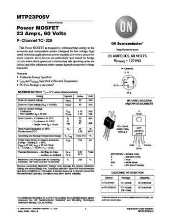
MTP23P06V Preferred Device Power MOSFET 23 Amps, 60 Volts P-Channel TO-220 This Power MOSFET is designed to withstand high energy in the http //onsemi.com avalanche and commutation modes. Designed for low voltage, high speed switching applications in power supplies, converters and power 23 AMPERES, 60 VOLTS motor controls, these devices are particularly well suited for bridge RDS(on)
mtp23p06vrev1e.pdf
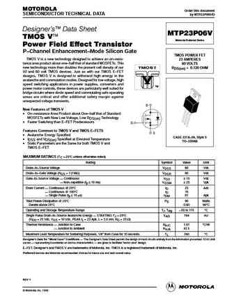
MOTOROLA Order this document SEMICONDUCTOR TECHNICAL DATA by MTP23P06V/D Designer's Data Sheet MTP23P06V TMOS V Motorola Preferred Device Power Field Effect Transistor P Channel Enhancement Mode Silicon Gate TMOS POWER FET TMOS V is a new technology designed to achieve an on resis- 23 AMPERES tance area product about one half that of standard MOSFETs. This 60 VOLTS
mtp2311m3.pdf
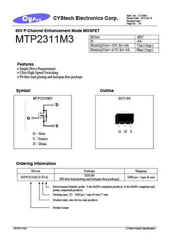
Spec. No. C733M3 Issued Date 2013.09.18 CYStech Electronics Corp. Revised Date Page No. 1/9 60V P-Channel Enhancement Mode MOSFET BVDSS -60V ID -4A MTP2311M3 RDSON@VGS=-10V, ID=-4A 72m (typ.) RDSON@VGS=-4.5V, ID=-3A 98m (typ.) Features Single Drive Requirement Ultra High Speed Switching Pb-free lead plating and halogen-free package Symbol Outlin
Otros transistores... MTP1N60 , MTP1N60E , MTP1N80E , MTP1N95 , MTP20N10E , MTP20N15EG , MTP20N20E , MTP20P06 , IRF520 , MTP23P06VG , MTP25N05E , MTP2955 , MTP2955V , MTP2N18 , MTP2N20 , MTP2N35 , MTP2N40 .
History: AP4501GH-HF | 2N65G-TN3-R | FTP10N60C | CM10N60AZ | 2N6796U
History: AP4501GH-HF | 2N65G-TN3-R | FTP10N60C | CM10N60AZ | 2N6796U
🌐 : EN ES РУ

Liste
Recientemente añadidas las descripciónes de los transistores:
MOSFET: AUB034N10 | AUB033N08BG | AUB026N085 | AUA062N08BG | AUA060N08AG | AUA056N08BGL | AUA039N10 | ASW80R290E | ASW65R120EFD | ASW65R110E | ASW65R095EFD | ASW65R046EFD | ASW65R041EFDA | ASW65R041E | ASW60R150E | ASW60R090EFDA
Popular searches
mrf450 | oc70 transistor | p0603bd mosfet | p157r5nt | ptp03n04n | sm4377 mosfet datasheet | tip31c reemplazo | 2sa906