IRFS630B MOSFET Equivalente. Reemplazo. Hoja de especificaciones. Principales características
Número de Parte: IRFS630B
Tipo de FET: MOSFET
Polaridad de transistor: N
ESPECIFICACIONES MÁXIMAS
Pdⓘ - Máxima disipación de potencia: 38 W
|Vds|ⓘ - Voltaje máximo drenador-fuente: 200 V
|Vgs|ⓘ - Voltaje máximo fuente-puerta: 30 V
|Id|ⓘ - Corriente continua de drenaje: 9 A
Tjⓘ - Temperatura máxima de unión: 150 °C
CARACTERÍSTICAS ELÉCTRICAS
trⓘ - Tiempo de subida: 70 nS
Cossⓘ - Capacitancia de salida: 85 pF
RDSonⓘ - Resistencia estado encendido drenaje a fuente: 0.4 Ohm
Encapsulados: TO220F
Búsqueda de reemplazo de IRFS630B MOSFET
- Selecciónⓘ de transistores por parámetros
IRFS630B datasheet
irf630b irfs630b.pdf
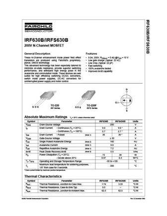
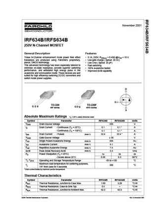
IRF630B/IRFS630B 200V N-Channel MOSFET General Description Features These N-Channel enhancement mode power field effect 9.0A, 200V, RDS(on) = 0.4 @VGS = 10 V transistors are produced using Fairchild s proprietary, Low gate charge ( typical 22 nC) planar, DMOS technology. Low Crss ( typical 22 pF) This advanced technology has been especially tailored to Fast switchin
irfs630a.pdf

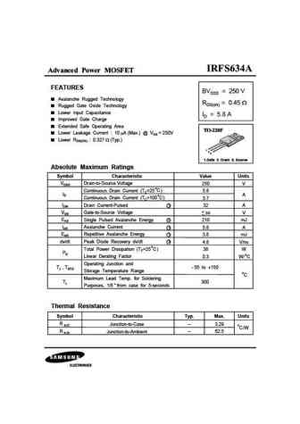
Advanced Power MOSFET FEATURES BVDSS = 200 V Avalanche Rugged Technology RDS(on) = 0.4 Rugged Gate Oxide Technology Lower Input Capacitance ID = 6.5 A Improved Gate Charge Extended Safe Operating Area Lower Leakage Current 10 A (Max.) @ VDS = 200V Low RDS(ON) 0.333 (Typ.) 1 2 3 1.Gate 2. Drain 3. Source Absolute Maximum Ratings Symbol Characteristic Valu

Otros transistores... IRFU430A , 12N65KL-TA , 12N65KL-TQ , 12N65KG-TA , 12N65KG-TF , 12N65KG-TQ , HY3306P , HY3306B , SKD502T , MT3203 , SVF5N60T , SVF5N60F , SVF5N60D , SVF5N60MJ , TSP5N60M , TSF5N60M , AO6414 .
History: HM15N50 | 2SK1638 | APT48M80L
History: HM15N50 | 2SK1638 | APT48M80L
🌐 : EN ES РУ

Liste
Recientemente añadidas las descripciónes de los transistores:
MOSFET: AUB062N08BG | AUB060N08AG | AUB056N10 | AUB056N08BGL | AUB050N085 | AUB050N055 | AUB045N12 | AUB045N10BT | AUB039N10 | AUB034N10 | AUB033N08BG | AUB026N085 | AUA062N08BG | AUA060N08AG | AUA056N08BGL | AUA039N10
Popular searches
c3199 transistor | 2n2712 datasheet | 2sc2525 | tip73 | 2n3392 | 2n2369a | 2sc733 | a933 transistor