IRFS630B Specs and Replacement
Type Designator: IRFS630B
Type of Transistor: MOSFET
Type of Control Channel: N-Channel
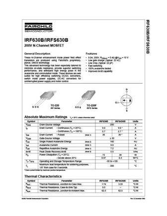
Absolute Maximum Ratings
Pd ⓘ - Maximum Power Dissipation: 38 W
|Vds|ⓘ - Maximum Drain-Source Voltage: 200 V
|Vgs|ⓘ - Maximum Gate-Source Voltage: 30 V
|Id| ⓘ - Maximum Drain Current: 9 A
Tj ⓘ - Maximum Junction Temperature: 150 °C
Electrical Characteristics
tr ⓘ - Rise Time: 70 nS
Cossⓘ - Output Capacitance: 85 pF
RDSonⓘ - Maximum Drain-Source On-State Resistance: 0.4 Ohm
Package: TO220F
IRFS630B substitution
- MOSFET ⓘ Cross-Reference Search
IRFS630B datasheet
irf630b irfs630b.pdf
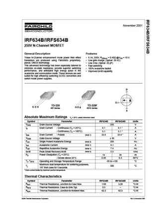
IRF630B/IRFS630B 200V N-Channel MOSFET General Description Features These N-Channel enhancement mode power field effect 9.0A, 200V, RDS(on) = 0.4 @VGS = 10 V transistors are produced using Fairchild s proprietary, Low gate charge ( typical 22 nC) planar, DMOS technology. Low Crss ( typical 22 pF) This advanced technology has been especially tailored to Fast switchin... See More ⇒
irfs630a.pdf

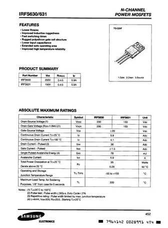
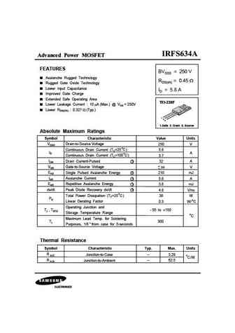
Advanced Power MOSFET FEATURES BVDSS = 200 V Avalanche Rugged Technology RDS(on) = 0.4 Rugged Gate Oxide Technology Lower Input Capacitance ID = 6.5 A Improved Gate Charge Extended Safe Operating Area Lower Leakage Current 10 A (Max.) @ VDS = 200V Low RDS(ON) 0.333 (Typ.) 1 2 3 1.Gate 2. Drain 3. Source Absolute Maximum Ratings Symbol Characteristic Valu... See More ⇒

Detailed specifications: IRFU430A, 12N65KL-TA, 12N65KL-TQ, 12N65KG-TA, 12N65KG-TF, 12N65KG-TQ, HY3306P, HY3306B, SKD502T, MT3203, SVF5N60T, SVF5N60F, SVF5N60D, SVF5N60MJ, TSP5N60M, TSF5N60M, AO6414
Keywords - IRFS630B MOSFET specs
IRFS630B cross reference
IRFS630B equivalent finder
IRFS630B pdf lookup
IRFS630B substitution
IRFS630B replacement
Need a MOSFET replacement? Our guide shows you how to find a perfect substitute by comparing key parameters and specs
History: 2SK1634 | JMSL0302AK
🌐 : EN ES РУ

LIST
Last Update
MOSFET: AUB062N08BG | AUB060N08AG | AUB056N10 | AUB056N08BGL | AUB050N085 | AUB050N055 | AUB045N12 | AUB045N10BT | AUB039N10 | AUB034N10
Popular searches
c3199 transistor | 2n2712 datasheet | 2sc2525 | tip73 | 2n3392 | 2n2369a | 2sc733 | a933 transistor