PJM3415PSA MOSFET Equivalente. Reemplazo. Hoja de especificaciones. Principales características
Número de Parte: PJM3415PSA
Tipo de FET: MOSFET
Polaridad de transistor: P
ESPECIFICACIONES MÁXIMAS
Pdⓘ - Máxima disipación de potencia: 1.5 W
|Vds|ⓘ - Voltaje máximo drenador-fuente: 20 V
|Vgs|ⓘ - Voltaje máximo fuente-puerta: 8 V
|Id|ⓘ - Corriente continua de drenaje: 4 A
Tjⓘ - Temperatura máxima de unión: 150 °C
CARACTERÍSTICAS ELÉCTRICAS
trⓘ - Tiempo de subida: 17 nS
Cossⓘ - Capacitancia de salida: 205 pF
RDSonⓘ - Resistencia estado encendido drenaje a fuente: 0.05 Ohm
Encapsulados: SOT23
Búsqueda de reemplazo de PJM3415PSA MOSFET
- Selecciónⓘ de transistores por parámetros
PJM3415PSA datasheet
pjm3415psa.pdf
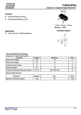
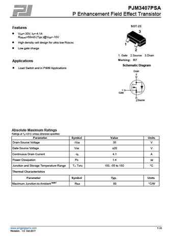
PJM3415PSA Silicon P-Channel Power MOSFET SOT-23 Features Low Gate Charge and RDS(on) ESD protected(HBM) up to 2KV 1. Gate 2.Source 3.Drain Marking 3415K Schematic Diagram Application Load switch and in PWM applications D G S Absolute Maximum Ratings Ratings at TA =25 unless otherwise specified. Parameter Symbol Maximum Units Drain-Source Voltage -V 20 V DS
pjm3400nsa.pdf
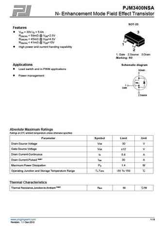
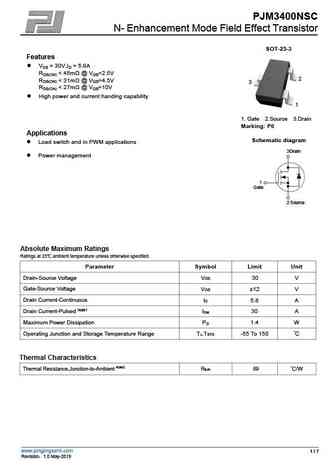
PJM3400NSA N- Enhancement Mode Field Effect Transistor SOT-23 Features VDS = 30V,ID = 5.8A RDS(ON)
pjm3401psc.pdf
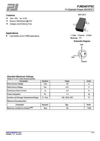
PJM3401PSC P-Channel Power MOSFET SOT-23-3 Features VDS= -30V I = -4.5A D RDS(ON)= 60m (max) @-10V 2 Halogen and Antimony Free 3 1 Applications 1. Gate 2.Source 3.Drain Load Switch and in PWM Applications Marking P1 Schematic Diagram Drain 3 1 Gate Source 2 Absolute Maximum Ratings Ratings at TA =25 unless otherwise specified. Parameter Symbol Valu
pjm3401psa.pdf
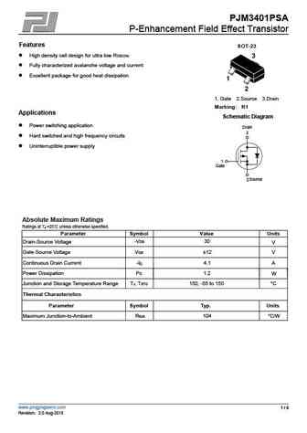
PJM3401PSA P-Enhancement Field Effect Transistor Features SOT-23 High density cell design for ultra low RDS(ON) Fully characterized avalanche voltage and current Excellent package for good heat dissipation 1. Gate 2.Source 3.Drain Marking R1 Applications Schematic Diagram Power switching application Drain 3 Hard switched and high frequency circuits Unint
Otros transistores... PJM2309PSA , PJM2309PSC , PJM2319PSA , PJM3400NSA , PJM3400NSC , PJM3401PSA , PJM3401PSC , PJM3407PSA , IRFP260 , PJM84PSA , EM6M2 , LSK3019FP8 , LSK3541FS8 , RD3P200SNFRA , RJU002N06 , RK7002BMHZG , RQ3C150BC .
🌐 : EN ES РУ

Liste
Recientemente añadidas las descripciónes de los transistores:
MOSFET: AUB034N10 | AUB033N08BG | AUB026N085 | AUA062N08BG | AUA060N08AG | AUA056N08BGL | AUA039N10 | ASW80R290E | ASW65R120EFD | ASW65R110E | ASW65R095EFD | ASW65R046EFD | ASW65R041EFDA | ASW65R041E | ASW60R150E | ASW60R090EFDA
Popular searches
irfp460 | irfz44n mosfet | lm317t datasheet | irf540 | bc337 | ksc1845 | c1815 transistor | 2sc1815