2310 MOSFET Equivalente. Reemplazo. Hoja de especificaciones. Principales características
Número de Parte: 2310
Tipo de FET: MOSFET
Polaridad de transistor: N
ESPECIFICACIONES MÁXIMAS
Pdⓘ - Máxima disipación de potencia: 0.35 W
|Vds|ⓘ - Voltaje máximo drenador-fuente: 60 V
|Vgs|ⓘ - Voltaje máximo fuente-puerta: 20 V
|Id|ⓘ - Corriente continua de drenaje: 3 A
Tjⓘ - Temperatura máxima de unión: 150 °C
CARACTERÍSTICAS ELÉCTRICAS
trⓘ - Tiempo de subida: 15 nS
Cossⓘ - Capacitancia de salida: 34 pF
RDSonⓘ - Resistencia estado encendido drenaje a fuente: 0.105 Ohm
Encapsulados: SOT23
Búsqueda de reemplazo de 2310 MOSFET
- Selecciónⓘ de transistores por parámetros
2310 datasheet
2310.pdf
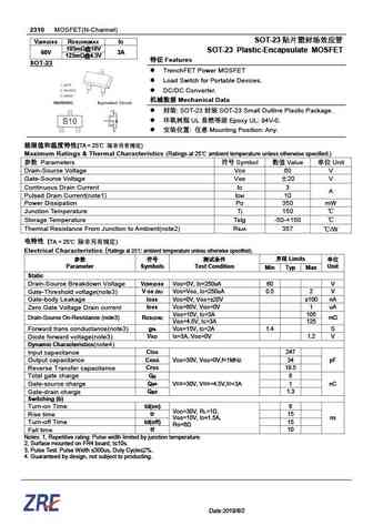
2310 MOSFET(N-Channel) SOT-23 V(BR)DSS RDS(ON)MAX ID 105m @10V SOT-23 Plastic-Encapsulate MOSFET 60V 3A 125m @4.5V Features SOT-23 TrenchFET Power MOSFET Load Switch for Portable Devices. DC/DC Converter. Mechanical Data SOT-23 SOT-23 Small Outline Plastic Package. UL Epoxy
st2310hi.pdf
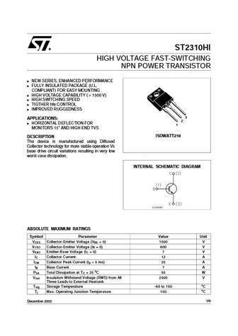
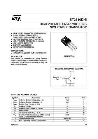
ST2310HI HIGH VOLTAGE FAST-SWITCHING NPN POWER TRANSISTOR NEW SERIES, ENHANCED PERFORMANCE FULLY INSULATED PACKAGE (U.L. COMPLIANT) FOR EASY MOUNTING HIGH VOLTAGE CAPABILITY ( > 1500 V) HIGH SWITCHING SPEED TIGTHER hfe CONTROL IMPROVED RUGGEDNESS 3 APPLICATIONS 2 HORIZONTAL DEFLECTION FOR 1 MONITORS 15" AND HIGH END TVS ISOWATT218 DESCRIPTION The device is manu
st2310dhi.pdf

ST2310DHI HIGH VOLTAGE FAST-SWITCHING NPN POWER TRANSISTOR NEW SERIES, ENHANCED PERFORMANCE FULLY INSULATED PACKAGE (U.L. COMPLIANT) FOR EASY MOUNTING INTEGRATED FREE WHEELING DIODE HIGH VOLTAGE CAPABILITY (> 1500 V) HIGH SWITCHING SPEED TIGTHER hfe CONTROL IMPROVED RUGGEDNESS 3 2 APPLICATIONS 1 HORIZONTAL DEFLECTION HIGH END TVS ISOWATT218 DESCRIPTION The devi
irl2310.pdf
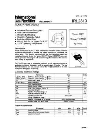
PD - 9.1275 PRELIMINARY IRL2310 HEXFET Power MOSFET Advanced Process Technology Ultra Low On-Resistance VDSS = 100V Dynamic dv/dt Rating Repetitive Avalanche Rated RDS(on) = 0.040 Logic-Level Gate Drive RDS(on) Specified at VGS= 4.5V & 10V 175 C Operating Temperature ID = 40A Description Fourth Generation HEXFETs from International Rectifier utilize advanced processing tech
md2310fx.pdf
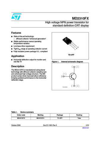
MD2310FX High voltage NPN power transistor for standard definition CRT display Features State-of-the-art technology diffused collector enhanced generation Stable performance versus operating temperature variation Low base drive requirement 3 2 Tight hFE range at operating collector current 1 Fully insulated power package U.L. compliant TO-3PF Appli
st2310dhi.pdf
ST2310DHI HIGH VOLTAGE FAST-SWITCHING NPN POWER TRANSISTOR NEW SERIES, ENHANCED PERFORMANCE FULLY INSULATED PACKAGE (U.L. COMPLIANT) FOR EASY MOUNTING INTEGRATED FREE WHEELING DIODE HIGH VOLTAGE CAPABILITY (> 1500 V) HIGH SWITCHING SPEED TIGTHER hfe CONTROL IMPROVED RUGGEDNESS 3 2 APPLICATIONS 1 HORIZONTAL DEFLECTION HIGH END TVS ISOWATT218 DESCRIPTION The devi
rn2310-rn2311.pdf
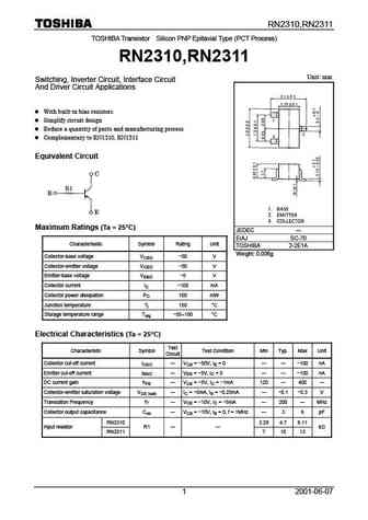
RN2310,RN2311 TOSHIBA Transistor Silicon PNP Epitaxial Type (PCT Process) RN2310,RN2311 Unit mm Switching, Inverter Circuit, Interface Circuit And Driver Circuit Applications With built-in bias resistors Simplify circuit design Reduce a quantity of parts and manufacturing process Complementary to RN1310, RN1311 Equivalent Circuit Maximum Ratings (Ta = 25 C) JEDE
ksc2310.pdf
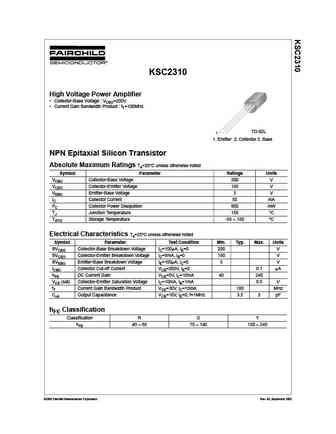
KSC2310 High Voltage Power Amplifier Collector-Base Voltage VCBO=200V Current Gain Bandwidth Product fT=100MHz TO-92L 1 1. Emitter 2. Collector 3. Base NPN Epitaxial Silicon Transistor Absolute Maximum Ratings Ta=25 C unless otherwise noted Symbol Parameter Ratings Units VCBO Collector-Base Voltage 200 V VCEO Collector-Emitter Voltage 150 V VEBO Emitter-Base Voltage 5
ksc2310.pdf
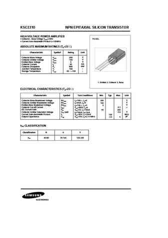
KSC2310 NPN EPITAXIAL SILICON TRANSISTOR HIGH VOLTAGE POWER AMPLIFIER Collector - Base Voltage VCBO=200V TO-92L Current Gain-Bandwidth Product fT=100MHz ABSOLUTE MAXIMUM RATINGS (TA=25 ) Characteristic Symbol Rating Unit V Collector-Base Voltage VCBO 200 V Collector-Emitter Voltage VCEO 150 V Emitter-Base Voltage VEBO 5 mA Collector Current IC 50 mW Collector Dissipation
sq2310es.pdf
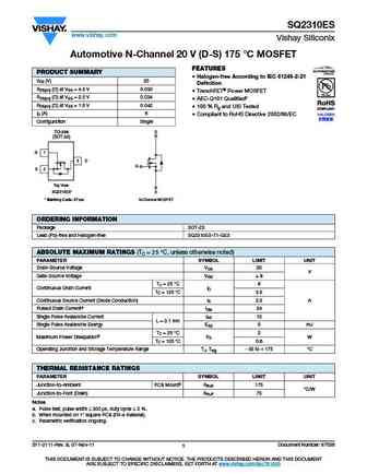
SQ2310ES www.vishay.com Vishay Siliconix Automotive N-Channel 20 V (D-S) 175 C MOSFET FEATURES PRODUCT SUMMARY Halogen-free According to IEC 61249-2-21 VDS (V) 20 Definition RDS(on) ( ) at VGS = 4.5 V 0.030 TrenchFET Power MOSFET RDS(on) ( ) at VGS = 2.5 V 0.034 AEC-Q101 Qualifiedc RDS(on) ( ) at VGS = 1.5 V 0.042 100 % Rg and UIS Tested ID (A) 6 Co
si2310b.pdf
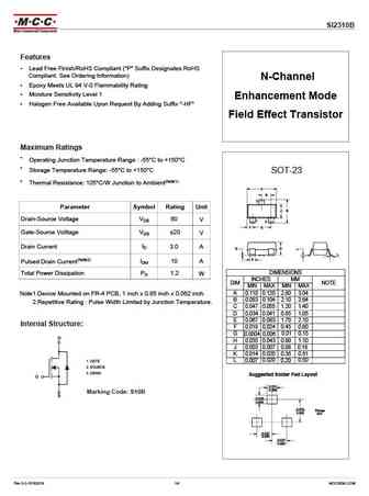
SI2310B Features Lead Free Finish/RoHS Compliant ("P" Suffix Designates RoHS Compliant. See Ordering Information) N-Channel Epoxy Meets UL 94 V-0 Flammability Rating Moisture Sensitivity Level 1 Enhancement Mode Halogen Free Available Upon Request By Adding Suffix "-HF" Field Effect Transistor Maximum Ratings Operating Junction Temperature Range -55 C to +150
si2310a.pdf
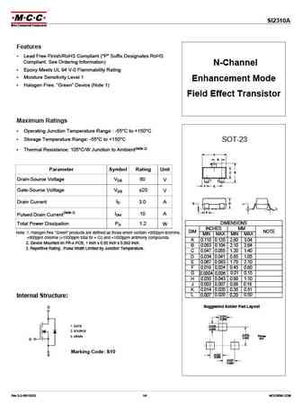
SI2310A Features Lead Free Finish/RoHS Compliant ("P" Suffix Designates RoHS Compliant. See Ordering Information) N-Channel Epoxy Meets UL 94 V-0 Flammability Rating Moisture Sensitivity Level 1 Enhancement Mode Halogen Free. Green Device (Note 1) Field Effect Transistor Maximum Ratings Operating Junction Temperature Range -55 C to +150 C Storage
si2310.pdf
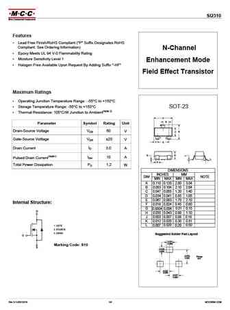
SI2310 Features Lead Free Finish/RoHS Compliant ("P" Suffix Designates RoHS Compliant. See Ordering Information) N-Channel Epoxy Meets UL 94 V-0 Flammability Rating Moisture Sensitivity Level 1 Enhancement Mode Halogen Free Available Upon Request By Adding Suffix "-HF" Field Effect Transistor Maximum Ratings Operating Junction Temperature Range -55 C to +150
2sc2310 2sc458.pdf
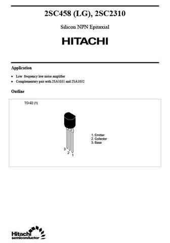
2SC458 (LG), 2SC2310 Silicon NPN Epitaxial Application Low frequency low noise amplifier Complementary pair with 2SA1031 and 2SA1032 Outline TO-92 (1) 1. Emitter 2. Collector 3. Base 3 2 1 2SC458 (LG), 2SC2310 Absolute Maximum Ratings (Ta = 25 C) Item Symbol 2SC458 (LG) 2SC2310 Unit Collector to base voltage VCBO 30 55 V Collector to emitter voltage VCEO 30 50 V Emit
smg2310a.pdf
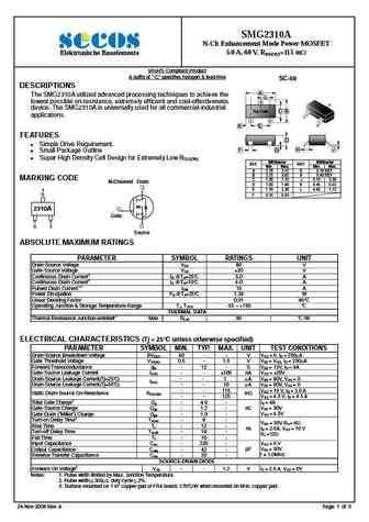
SMG2310A N-Ch Enhancement Mode Power MOSFET 5.0 A, 60 V, RDS(ON)=115 m Elektronische Bauelemente sRoHS Compliant Product A suffix of -C specifies halogen & lead-free SC-59 DESCRIPTIONS A The SMG2310A utilized advanced processing techniques to achieve the L lowest possible on-resistance, extremely efficient and cost-effectiveness 3 3 device. The SMG2310A is univers
smg2310n.pdf
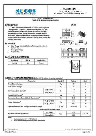
SMG2310N 2.2A, 30V, RDS(ON) 65 m N-Channel Enhancement Mode MOSFET Elektronische Bauelemente RoHS Compliant Product A suffix of -C specifies halogen and lead-free SC-59 DESCRIPTION These miniature surface mount MOSFETs utilize High Cell A Density process. Low RDS(on) assures minimal power loss and L conserves energy, making this device ideal for use in power 3 3
sgm2310a.pdf
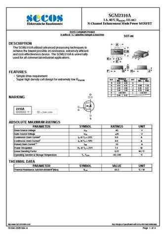
SGM2310A 5 A, 60 V, RDS(ON) 115 m N-Channel Enhancement Mode Power MOSFET Elektronische Bauelemente RoHS Compliant Product A suffix of -C specifies halogen & lead-free SOT-89 DESCRIPTION A The SGM2310A utilized advanced processing techniques to 4 achieve the lowest possible on-resistance, extremely efficient Top View C B and cost-effectiveness device. The SGM231
tsm2310cx.pdf
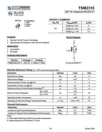
TSM2310 20V N-Channel MOSFET PRODUCT SUMMARY SOT-23 Pin Definition 1. Gate VDS (V) RDS(on)(m ) ID (A) 2. Source 33 @ VGS = 4.5V 4 3. Drain 20 40 @ VGS = 2.5V 3.2 100 @ VGS = 1.8V 2.0 Features Block Diagram Advance Trench Process Technology High Density Cell Design for Ultra Low On-resistance Application Load Switch PA Switch Ordering Info
cj2310.pdf
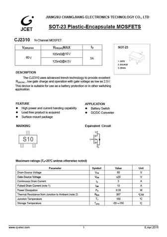
JIANGSU CHANGJIANG ELECTRONICS TECHNOLOGY CO., LTD SOT-23 Plastic-Encapsulate MOSFETS CJ2310 N-Channel MOSFET ID SOT-23 V(BR)DSS RDS(on)MAX 105m @10V 60 V 3A 1. GATE 125m @4.5V 2. SOURCE 3. DRAIN DESCRIPTION The CJ2310 uses advanced trench technology to provide excellent RDS(ON) , low gate charge and operation with gate voltage as low as 2.5V. This device is s
ku2310q.pdf
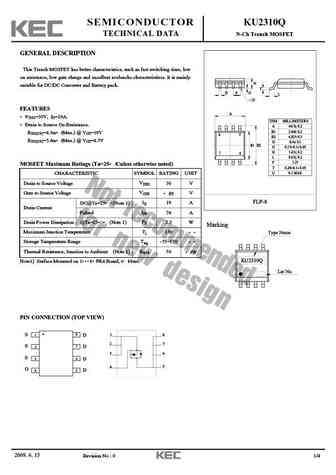
SEMICONDUCTOR KU2310Q TECHNICAL DATA N-Ch Trench MOSFET GENERAL DESCRIPTION This Trench MOSFET has better characteristics, such as fast switching time, low on resistance, low gate charge and excellent avalanche characteristiscs. It is mainly H suitable for DC/DC Converter and Battery pack. T D P G L U FEATURES A VDSS=30V, ID=19A. DIM MILLIMETERS Drain to Source On Resistance
ceh2310.pdf
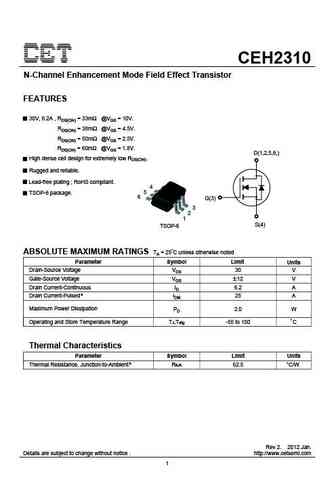
CEH2310 N-Channel Enhancement Mode Field Effect Transistor FEATURES 30V, 6.2A , RDS(ON) = 33m @VGS = 10V. RDS(ON) = 38m @VGS = 4.5V. RDS(ON) = 50m @VGS = 2.5V. RDS(ON) = 60m @VGS = 1.8V. D(1,2,5,6,) High dense cell design for extremely low RDS(ON). Rugged and reliable. Lead-free plating ; RoHS compliant. 4 5 TSOP-6 package. 6 G(3) 3 2 1 S(4) TSOP-6 ABSOLUTE
ces2310.pdf
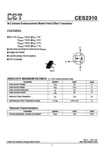
CES2310 N-Channel Enhancement Mode Field Effect Transistor FEATURES 30V, 4.8A, RDS(ON) = 34m @VGS = 10V. RDS(ON) = 38m @VGS = 4.5V. RDS(ON) = 50m @VGS = 2.5V. RDS(ON) = 60m @VGS = 1.8V. D High dense cell design for extremely low RDS(ON). Rugged and reliable. Lead-free plating ; RoHS compliant. SOT-23 package. G D S G S SOT-23 ABSOLUTE MAXIMUM RATINGS TA = 25 C u
wtm2310a.pdf
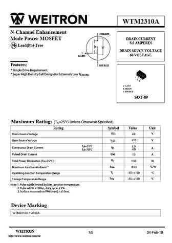
WTM2310A N-Channel Enhancement 3 DRAIN Mode Power MOSFET DRAIN CURRENT 5.0 AMPERES P b Lead(Pb)-Free DRAIN SOUCE VOLTAGE 1 60 VOLTAGE GATE Features 2 SOURCE * Simple Drive Requirement. * Super High Density Cell Design for Extremely Low RDS(ON). 1 2 3 1. GATE 2. DRAIN 3. SOURCE SOT-89 Maximum Ratings (TA=25 C Unless Otherwise Specified) Rating Symbol Value Unit VDS V D
aons32310.pdf
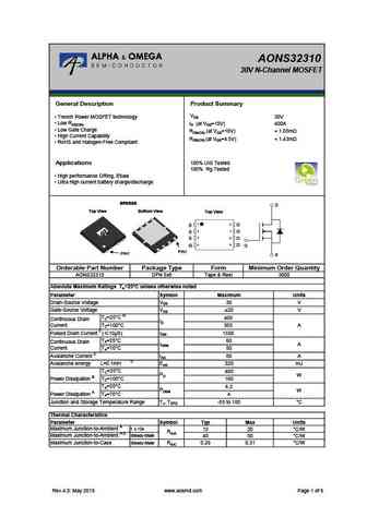
AONS32310 30V N-Channel MOSFET General Description Product Summary VDS Trench Power MOSFET technology 30V Low RDS(ON) ID (at VGS=10V) 400A Low Gate Charge RDS(ON) (at VGS=10V)
ap2310gg-hf.pdf
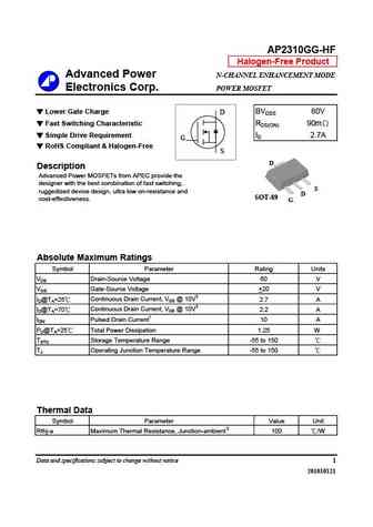
AP2310GG-HF Halogen-Free Product Advanced Power N-CHANNEL ENHANCEMENT MODE Electronics Corp. POWER MOSFET Lower Gate Charge BVDSS 60V D Fast Switching Characteristic RDS(ON) 90m Simple Drive Requirement ID 2.7A G RoHS Compliant & Halogen-Free S D Description Advanced Power MOSFETs from APEC provide the designer with the best combination of fast switching, S rug
ap2310gk-hf.pdf
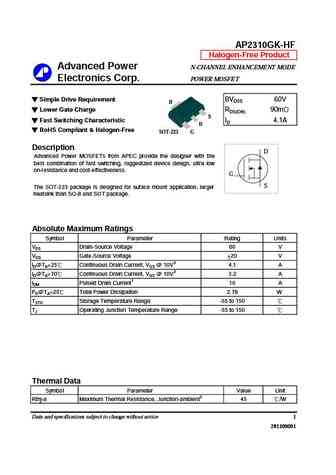
AP2310GK-HF Halogen-Free Product Advanced Power N-CHANNEL ENHANCEMENT MODE Electronics Corp. POWER MOSFET Simple Drive Requirement BVDSS 60V D Lower Gate Charge RDS(ON) 90m S Fast Switching Characteristic ID 4.1A D RoHS Compliant & Halogen-Free SOT-223 G Description D Advanced Power MOSFETs from APEC
ap2310cgn-hf.pdf
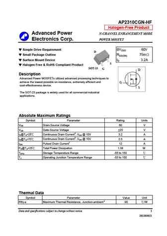
AP2310CGN-HF Halogen-Free Product Advanced Power N-CHANNEL ENHANCEMENT MODE Electronics Corp. POWER MOSFET Simple Drive Requirement BVDSS 60V D Small Package Outline RDS(ON) 75m Surface Mount Device ID 3.2A S Halogen Free & RoHS Compliant Product SOT-23 G D Description Advanced Power MOSFETs utilized advanced processing techniques to achieve the lowest possible
ap2310agn-hf.pdf
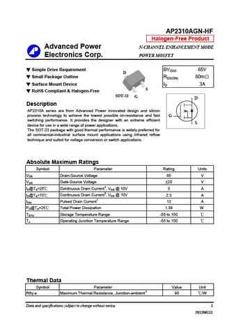
AP2310AGN-HF Halogen-Free Product Advanced Power N-CHANNEL ENHANCEMENT MODE Electronics Corp. POWER MOSFET Simple Drive Requirement BVDSS 65V D Small Package Outline RDS(ON) 80m Surface Mount Device ID 3A S RoHS Compliant & Halogen-Free SOT-23 G D Description AP2310A series are from Advanced Power innovated design and silicon process technology to achieve the lo
ap2310gn-hf.pdf
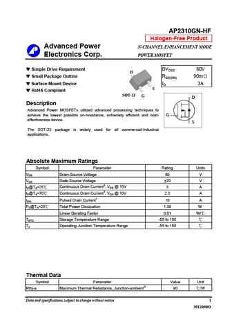
AP2310GN-HF Halogen-Free Product Advanced Power N-CHANNEL ENHANCEMENT MODE Electronics Corp. POWER MOSFET Simple Drive Requirement BVDSS 60V D Small Package Outline RDS(ON) 90m Surface Mount Device ID 3A S RoHS Compliant SOT-23 G D Description Advanced Power MOSFETs utilized advanced processing techniques to achieve the lowest possible on-resistance, extremely e
ap2310gn.pdf
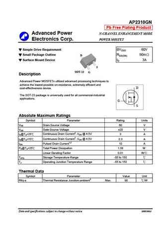
AP2310GN Pb Free Plating Product Advanced Power N-CHANNEL ENHANCEMENT MODE Electronics Corp. POWER MOSFET Simple Drive Requirement BVDSS 60V Small Package Outline RDS(ON) 90m D Surface Mount Device ID 3A S SOT-23 G Description Advanced Power MOSFETs utilized advanced processing techniques to achieve the lowest possible o
am2310n.pdf
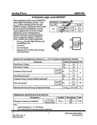
Analog Power AM2310N N-Channel Logic Level MOSFET These miniature surface mount MOSFETs PRODUCT SUMMARY utilize High Cell Density process. Low rDS(on) assures minimal power loss and VDS (V) rDS(on) ( )ID (A) conserves energy, making this device ideal 0.065 @ VGS = 4.5V 2.2 for use in power management circuitry. 30 0.082 @ VGS = 2.5V 2.0 Typical applications are lower voltage
si2310.pdf
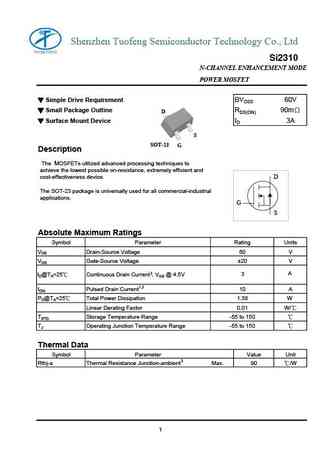
Shenzhen Tuofeng Semiconductor Technology Co., Ltd Si2310 N-CHANNEL ENHANCEMENT MODE POWER MOSFET Simple Drive Requirement BVDSS 60V Small Package Outline RDS(ON) 90m D Surface Mount Device ID 3A S SOT-23 G Description The MOSFETs utilized advanced processing techniques to achieve the lowest possible on-resistance,
mtn2310v8.pdf
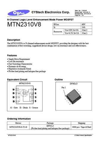
Spec. No. C393V8 Issued Date 2013.06.13 CYStech Electronics Corp. Revised Date 2013.06.24 Page No. 1/9 N-Channel Logic Level Enhancement Mode Power MOSFET BVDSS 60V MTN2310V8 ID 14A 31m VGS=10V, ID=3A RDSON(TYP) 35m VGS=4.5V, ID=2A Description The MTN2310V8 is a N-channel enhancement-mode MOSFET, providing the designer with the best combination of fast s
mtn2310m3.pdf
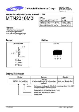
Spec. No. C393M3 Issued Date 2007.05.28 CYStech Electronics Corp. Revised Date 2015.09.02 Page No. 1/9 60V N-Channel Enhancement Mode MOSFET BVDSS 60V MTN2310M3 ID@VGS=10V, TA=25 C 4.8A RDSON@VGS=10V, ID=4A 41m (typ) RDSON@VGS=5V, ID=3A 46m (typ) Features Simple drive requirement Small package outline Pb-free lead plating package Symbol Outline
mtn2310n3.pdf
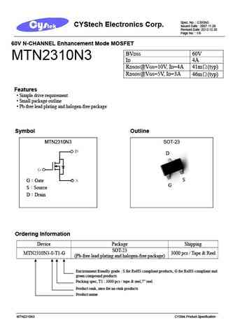
Spec. No. C393N3 CYStech Electronics Corp. Issued Date 2007.11.26 Revised Date 2013.12.30 Page No. 1/9 60V N-CHANNEL Enhancement Mode MOSFET BVDSS 60V MTN2310N3 ID 4A RDSON@VGS=10V, ID=4A 41m (typ) RDSON@VGS=5V, ID=3A 46m (typ) Features Simple drive requirement Small package outline Pb-free lead plating and halogen-free package Symbol Outline MT
sm2310nsa.pdf
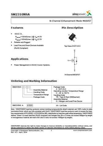
SM2310NSA N-Channel Enhancement Mode MOSFET Features Pin Description 55V/2.1A , D RDS(ON)=130m (max.) @ VGS=4.5V S RDS(ON)=180m (max.) @ VGS=2.5V G Reliable and Rugged Lead Free and Green Devices Available Top View of SOT-23-3 (RoHS Compliant) D Applications G Power Management in DC/AC Inverer Systems. S N-Channel MOSFET Ordering and Marking Information SM2310NS Pac
ftk2310.pdf
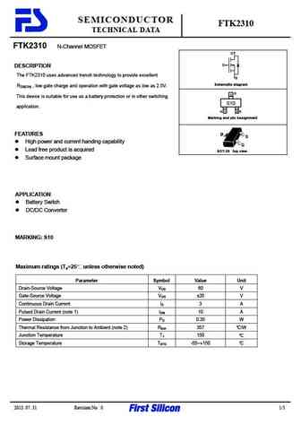
SEMICONDUCTOR FTK2310 TECHNICAL DATA FTK2310 N-Channel MOSFET D G DESCRIPTION The FTK2310 uses advanced trench technology to provide excellent S Schematic diagram RDS(ON) , low gate charge and operation with gate voltage as low as 2.5V. D 3 This device is suitable for use as a battery protection or in other switching S10 application. G 1 2 S Marking and pin Assignment F
ki2310.pdf
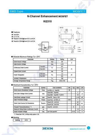
SMD Type MOSFET N-Channel Enhancement MOSFET KI2310 SOT-23 Unit mm +0.1 2.9-0.1 +0.1 0.4 -0.1 Features 3 VDS=20V ID = 6 .5A RDS(on)= 22m @VGS=4.5V ,ID=6.5A 1 2 RDS(on)= 30m @VGS=2.5V ,ID=5.5A +0.05 0.95+0.1 -0.1 0.1 -0.01 1.9+0.1 -0.1 G 1 3 D 1.Gate S 2 2.Source 3.Drain Absolute Maximum Ratings Ta = 25 Parameter Symbol Rating Unit Dr
ki2310ds.pdf
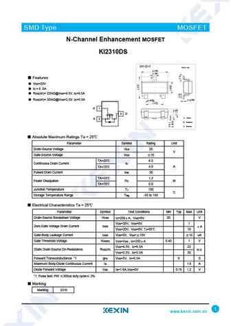
SMD Type MOSFET N-Channel Enhancement MOSFET KI2310DS SOT-23-3 Unit mm +0.2 2.9 -0.1 +0.1 0.4-0.1 3 Features VDS=20V ID = 6 .5A RDS(on)= 22m @VGS=4.5V ,ID=6.5A 1 2 +0.02 +0.1 RDS(on)= 30m @VGS=2.5V ,ID=5.5A 0.15 -0.02 0.95 -0.1 +0.1 1.9 -0.2 G 1 3 D 1. Gate S 2 2. Source 3. Drain Absolute Maximum Ratings Ta = 25 Parameter Symbol Rati
chm2310gp.pdf
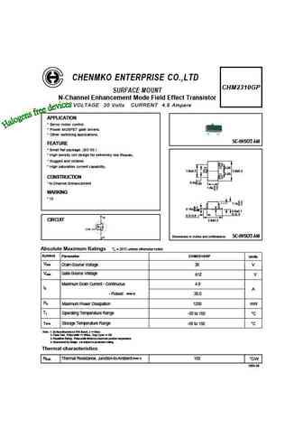
CHENMKO ENTERPRISE CO.,LTD CHM2310GP SURFACE MOUNT N-Channel Enhancement Mode Field Effect Transistor VOLTAGE 30 Volts CURRENT 4.8 Ampere APPLICATION * Servo motor control. * Power MOSFET gate drivers. * Other switching applications. SC-59/SOT-346 FEATURE * Small flat package. (SC-59 ) * High density cell design for extremely low RDS(ON). * Rugged and reliable. * High saturati
shd231009.pdf
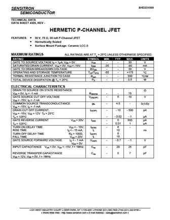
SHD231009 SENSITRON SEMICONDUCTOR TECHNICAL DATA DATA SHEET 4305, REV - HERMETIC P-CHANNEL JFET FEATURES 30 V, 75 , 30 mA P-Channel JFET Hermetically Sealed Surface Mount Package Ceramic LCC-3 MAXIMUM RATINGS ALL RATINGS ARE AT TA = 25 C UNLESS OTHERWISE SPECIFIED. RATING SYMBOL MIN. TYP. MAX. UNITS GATE TO SOURCE VOLTAGE ID = 1 A, VDS = 0V VGS - - 30 V
shd231006.pdf
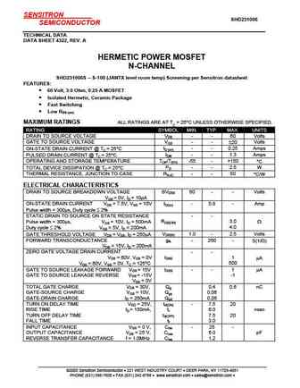
SENSITRON SHD231006 SEMICONDUCTOR TECHNICAL DATA DATA SHEET 4322, REV. A HERMETIC POWER MOSFET N-CHANNEL SHD231006S -- S-100 (JANTX level room temp) Screening per Sensitron datasheet FEATURES 60 Volt, 3.0 Ohm, 0.25 A MOSFET Isolated Hermetic, Ceramic Package Fast Switching Low RDS (on) MAXIMUM RATINGS ALL RATINGS ARE AT TC = 25 C UNLESS OTHERWISE SPEC
shd231008.pdf
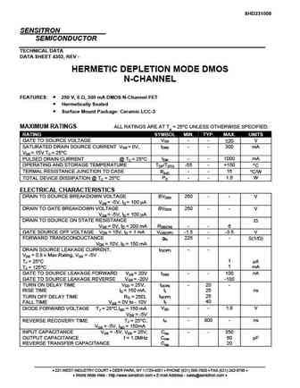
SHD231008 SENSITRON SEMICONDUCTOR TECHNICAL DATA DATA SHEET 4302, REV - HERMETIC DEPLETION MODE DMOS N-CHANNEL FEATURES 250 V, 6 , 300 mA DMOS N-Channel FET Hermetically Sealed Surface Mount Package Ceramic LCC-3 MAXIMUM RATINGS ALL RATINGS ARE AT TA = 25 C UNLESS OTHERWISE SPECIFIED. RATING SYMBOL MIN. TYP. MAX. UNITS GATE TO SOURCE VOLTAGE VGS - - 2
ssm2310gn.pdf
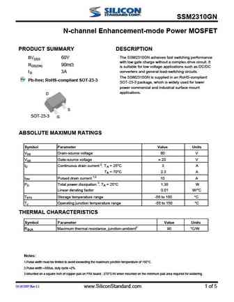
SSM2310GN N-channel Enhancement-mode Power MOSFET PRODUCT SUMMARY DESCRIPTION The SSM2310GN acheives fast switching performance BVDSS 60V with low gate charge without a complex drive circuit. It RDS(ON) 90m is suitable for low voltage applications such as DC/DC converters and general load-switching circuits. I 3A D The SSM2310GN is supplied in an RoHS-compliant Pb-free; RoHS-com
si2310a.pdf
R UMW UMW SI2310A UMW SI2310A UMW SI2310A N-ChanneI Power MOSFET Features SOT 23 Simple Drive Requirement Small Package Outline Surface Mount Device 1. GATE 2. SOURCE 3. DRAIN MARKING D G MS10 S Absolute Maximum Ratings Ta = 25 Parameter Symbol Rating Unit Drain-Source Voltage VD S 60 V GS Gate-Source Voltage V 20 V A Continuous Drain Current
atm2310nsa.pdf
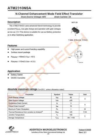
ATM2310NSA N-Channel Enhancement Mode Field Effect Transistor Drain-Source Voltage 60V Drain Current 3A Description The ATM2310NSA uses advanced trench technology to provide excellent R , low gate charge and operation with gate voltages DS(ON) as low as 2.5V.This device is suitable for use as Battery protection or in other Switching application. Features High power and current h
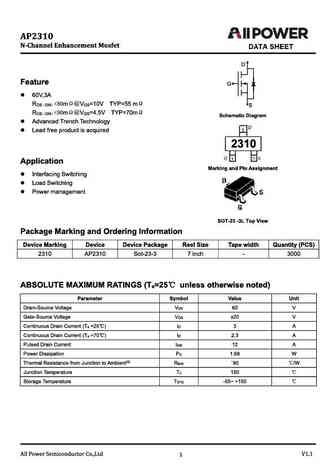
ap2310s.pdf
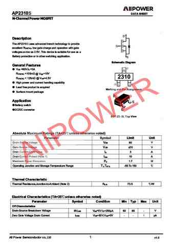
AIIP ER AP2310S DATA SHEET N-Channel p wer MOSFET Descripti n The AP2310S uses advanced trench technol y to provide N low gate charge and operation with gate excellent Rosco , voltages as low as 2.5V. This device is suitable for use as a Ba e protection or in other switching application. Schematic Diagram General Features 3A Vos =60V o = ,l Ros(ON
as2310.pdf
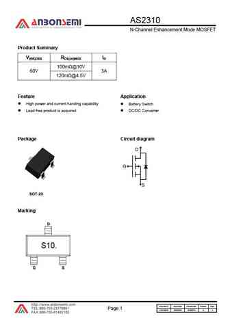
AS2310 N-Channel Enhancement Mode MOSFET Product Summary V(BR)DSS RDS(on)MAX ID 100m @10V 60V 3A 120m @4.5V Feature Application High power and current handing capability Battery Switch Lead free product is acquired DC/DC Converter Package Circuit diagram SOT-23 Marking S10. Document ID Issued Date Revised Date Revision Page. Page 1 AS-3150040 2003/03/08 2018
as2310a.pdf
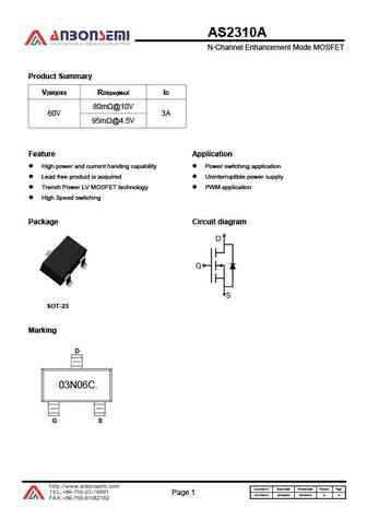
AS2310A N-Channel Enhancement Mode MOSFET Product Summary V R I (BR)DSS DS(on)MAX D 80m @10V 60V 3A 95m @4.5V Feature Application High power and current handing capability Power switching application Lead free product is acquired Uninterruptible power supply Trench Power LV MOSFET technology PWM application High Speed switching Package Circuit diagram
si2310.pdf
SI2310 MOSFET ROHS N-Channel Enhancement-Mode MOSFET SOT-23 - Features Advanced trench process technology High Density Cell Design For Ultra Low On-Resistance High Power and Current handing capability MAXIMUM RANTINGS Parameter Symbol Ratings Unit Drain-Source Voltage VDSS 60 V Gate-Source Voltage VGSS 16 Drain Current (Note 1) ID 3.8 A Power Dissipation (N
hss2310a.pdf
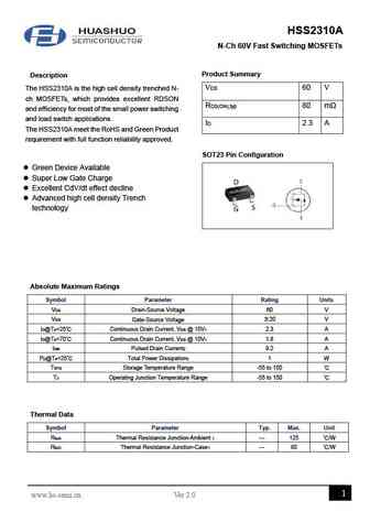
HSS2310A N-Ch 60V Fast Switching MOSFETs Product Summary Description VDS 60 V The HSS2310A is the high cell density trenched N- ch MOSFETs, which provides excellent RDSON RDS(ON),typ 80 m and efficiency for most of the small power switching and load switch applications. ID 2.3 A The HSS2310A meet the RoHS and Green Product requirement with full function reliability appr
hd2310.pdf
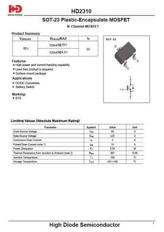
HD2310 SOT-23 Plastic-Encapsulate MOSFET N -Channel MOSFET roduct Summary P ID V(BR)DSS RDS(on)MAX SOT- 23 105m @10V D 60 V 3A 125m @4.5V S Features High power and current handing capability G Lead free product is acquired Surface mount package Applications DC/DC Converters Battery Switch Marking S10 Parameter Symbol Va
jmty2310a.pdf
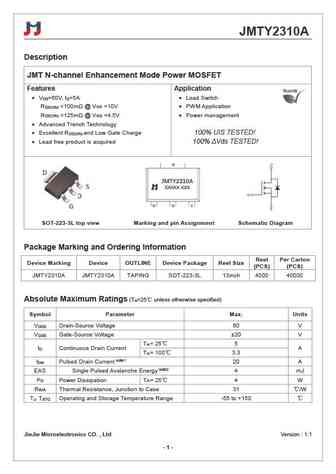
JMTY2310A Description JMT N-channel Enhancement Mode Power MOSFET Features Application V =60V, I =5A Load Switch DS D R
jmtm2310a.pdf
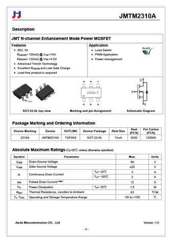
JMTM2310A Description JMT N-channel Enhancement Mode Power MOSFET Features Application 60V, 3A Load Switch R
jmtn2310a.pdf
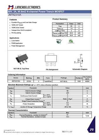
60V, 3A, 95.6m N-channel Power Trench MOSFET JMTN2310A Product Summary Features Excellent RDS(ON) and Low Gate Charge Parameters Value Unit 100% UIS Tested VDSS 60 V 100% Vds Tested VGS(th)_Typ 1.6 V Halogen-free; RoHS-compliant ID(@VGS=10V) 3 A Pb-free plating RDS(ON)_Typ(@VGS=10V 85.0 mW RDS(ON)_Typ(@VGS=4.5V 95.6 mW Applications Load Switch P
jmtl2310a.pdf
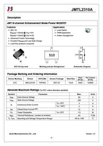
JMTL2310A Description JMT N-channel Enhancement Mode Power MOSFET Features Application 60V, 3A Load Switch R
si2310.pdf
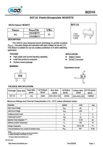
SI2310 SOT-23 Plastic-Encapsulate MOSFETS SOT-23 30V N-Channel MOSFET 3 ID Max V(BR)DSS RDS(on)Typ 105m @10V 1. GATE 3A 60V 2. SOURCE 125m @4.5V 1 3. DRAIN 2 DESCRIPTION The SI2310 uses advanced trench technology to provide excellent RDS(ON) , low gate charge and operation with gate voltage as low as 2.5V. This device is suitable for use as a battery prote
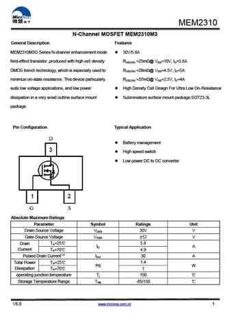
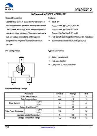
mem2310m3.pdf
MEM2310 N-Channel MOSFET MEM2310M3 General Description Features MEM2310M3G Series N-channel enhancement mode 30V/5.8A field-effect transistor ,produced with high cell density RDS(ON) =25m @ VGS=10V, ID=5.8A DMOS trench technology, which is especially used to RDS(ON) =28m @ VGS=4.5V, ID=5A minimize on-state resistance. This device particularly RDS(ON) =37m @ VGS=2.5V, ID=4A
mem2310x.pdf
MEM2310 N-Channel MOSFET MEM2310X General Description Features MEM2310XG Series N-channel enhancement mode 30V/5.8A field-effect transistor ,produced with high cell density RDS(ON) =25m @ VGS=10V, ID=5.8A DMOS trench technology, which is especially used to RDS(ON) =28m @ VGS=4.5V, ID=5A minimize on-state resistance. This device particularly RDS(ON) =37m @ VGS=2.5V, ID=4A s
si2310.pdf
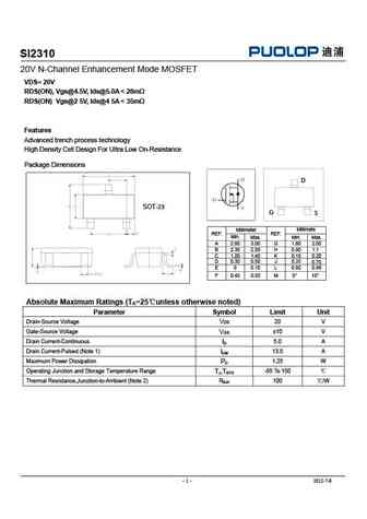
SI2310 20V N-Channel Enhancement Mode MOSFET VDS= 20V RDS(ON), Vgs@4.5V, Ids@5.0A
sk2310aa.pdf
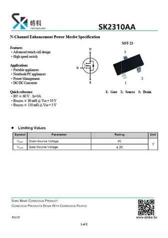
N-Channel Enhancement Power Mosfet Specification Power Mosfet Specification SOT-23 Features Advanced trench cell design 3 High speed switch Applications Portable appliances Notebook/PC appliances Power Management 2 DC/DC Converter 1 Quick reference 1 Gate 2 Gate 2 Source 3 Drain BV 60 V ID=3A RDS(ON) 90 m @ VGS = 10 V RDS(ON) 11
tf2310.pdf
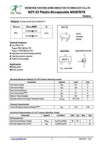
SHENZHEN TUOFENG SEMICONDUCTOR TECHNOLOGY CO.,LTD SOT-23 Plastic-Encapsulate MOSFETS TF2310 N-Channel 60-V(D-S) MOSFET TF2310 V(BR)DSS RDS(on)MAX ID SOT-23 0.090 @ 10V 3 60V 3.0 A 1.GATE 0.120 @ 4.5 V 2.SOURCE 3.DRAIN 1 2 General Features VDS =60V,ID =3A RDS(ON)
si2310.pdf
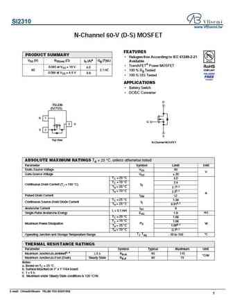
SI2310 www.VBsemi.tw N-Channel 60-V (D-S) MOSFET FEATURES PRODUCT SUMMARY Halogen-free According to IEC 61249-2-21 VDS (V) RDS(on) ( ) ID (A)a Qg (Typ.) Available TrenchFET Power MOSFET 0.085 at VGS = 10 V 4.0 60 2.1 nC 100 % Rg Tested 0.096 at VGS = 4.5 V 3.8 100 % UIS Tested APPLICATIONS Battery Switch DC/DC Converter D TO-236 (SOT23) G 1
ap2310gg.pdf
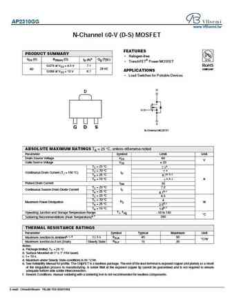
AP2310GG www.VBsemi.tw N-Channel 60-V (D-S) MOSFET FEATURES PRODUCT SUMMARY Halogen-free VDS (V) RDS(on) ( ) ID (A)a Qg (Typ.) TrenchFET Power MOSFET 0.076 at VGS = 4.5 V 7.1 RoHS 29 nC COMPLIANT 60 APPLICATIONS 0.088 at VGS = 10 V 6.7 Load Switches for Portable Devices D D G S G D S N-Channel MOSFET ABSOLUTE MAXIMUM RATINGS TA = 25 C, unless otherwise n
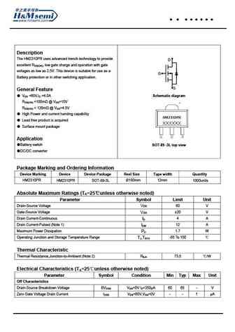
hm2310pr.pdf
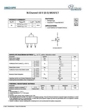
HM2310PR www.VBsemi.tw N-Channel 60-V (D-S) MOSFET FEATURES PRODUCT SUMMARY Halogen-free VDS (V) RDS(on) ( ) ID (A)a Qg (Typ.) TrenchFET Power MOSFET 0.076 at VGS = 4.5 V 7.1 RoHS 29 nC COMPLIANT 60 APPLICATIONS 0.088 at VGS = 10 V 6.7 Load Switches for Portable Devices D D G S G D S N-Channel MOSFET ABSOLUTE MAXIMUM RATINGS TA = 25 C, unless otherwise n
hm2310.pdf
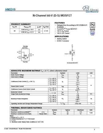
HM2310 www.VBsemi.tw N-Channel 60-V (D-S) MOSFET FEATURES PRODUCT SUMMARY Halogen-free According to IEC 61249-2-21 VDS (V) RDS(on) ( ) ID (A)a Qg (Typ.) Available TrenchFET Power MOSFET 0.085 at VGS = 10 V 4.0 60 2.1 nC 100 % Rg Tested 0.096 at VGS = 4.5 V 3.8 100 % UIS Tested APPLICATIONS Battery Switch DC/DC Converter D TO-236 (SOT23) G 1
kd2310.pdf

KD2310 www.VBsemi.tw N-Channel 60-V (D-S) MOSFET FEATURES PRODUCT SUMMARY Halogen-free According to IEC 61249-2-21 VDS (V) RDS(on) ( ) ID (A)a Qg (Typ.) Available TrenchFET Power MOSFET 0.085 at VGS = 10 V 4.0 60 2.1 nC 100 % Rg Tested 0.096 at VGS = 4.5 V 3.8 100 % UIS Tested APPLICATIONS Battery Switch DC/DC Converter D TO-236 (SOT23) G 1
me2310.pdf
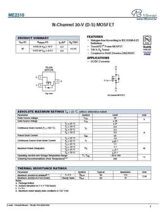
ME2310 www.VBsemi.tw N-Channel 30-V (D-S) MOSFET FEATURES PRODUCT SUMMARY Halogen-free According to IEC 61249-2-21 VDS (V) RDS(on) ( ) ID (A)a Qg (Typ.) Definition 0.030 at VGS = 10 V TrenchFET Power MOSFET 6.5 30 4.5 nC 100 % Rg Tested 0.033 at VGS = 4.5 V 6.0 Compliant to RoHS Directive 2002/95/EC APPLICATIONS DC/DC Converter D TO-236 (SOT-23) G 1
hm2310b.pdf

HM2310B N Channel Enhancement Mode MOSFET DESCRIPTION The HM2310B is the N-Channel logic enhancement mode power field effect transistor is produced using high cell density, DMOS trench technology. This high-density process is especially tailored to minimize on-state resistance. These devices are particularly suited for low voltage application such as cellular phone and notebook co
hm2310pr.pdf
HM2310PR Description The HM2310PR uses advanced trench technology to provide D excellent RDS(ON), low gate charge and operation with gate voltages as low as 2.5V. This device is suitable for use as a G Battery protection or in other switching application. S General Feature VDS =60V,ID =4.0A Schematic diagram RDS(ON)
hm2310.pdf
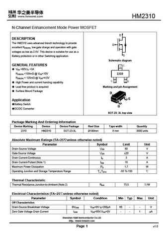
HM2310 N-Channel Enhancement Mode Power MOSFET D DESCRIPTION The HM2310 uses advanced trench technology to provide G excellent RDS(ON), low gate charge and operation with gate voltages as low as 2.5V. This device is suitable for use as a S Battery protection or in other Switching application. Schematic diagram GENERAL FEATURES VDS =60V,ID =3A RDS(ON)
hm2310c.pdf
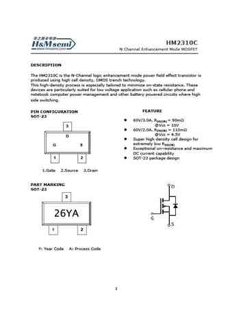
HM N Channel Enhancement Mode MOSFET DESCRIPTION The HM2310C is the N-Channel logic enhancement mode power field effect transistor is produced using high cell density, DMOS trench technology. This high-density process is especially tailored to minimize on-state resistance. These devices are particularly suited for low voltage application such as cellular phone and notebook co
Otros transistores... TX40N06B , TX50N06 , XG65T125PS1B , XG65T230PS1B , XGP6508B , XGP6510B , YWNM6001 , 2N7002AK , IRLB4132 , 3407 , SPA22N65G , SPA24N50G , SPA65R38G , SPA65R72G , SPC10N65G , SPC10N80G , SPC16N65G .
History: VS8205BH
History: VS8205BH
🌐 : EN ES РУ

Liste
Recientemente añadidas las descripciónes de los transistores:
MOSFET: AUB034N10 | AUB033N08BG | AUB026N085 | AUA062N08BG | AUA060N08AG | AUA056N08BGL | AUA039N10 | ASW80R290E | ASW65R120EFD | ASW65R110E | ASW65R095EFD | ASW65R046EFD | ASW65R041EFDA | ASW65R041E | ASW60R150E | ASW60R090EFDA
Popular searches
2sc828 replacement | 2sd669 datasheet | c102 transistor | bt152 datasheet | 2sa1302 datasheet | mpsa13 transistor equivalent | кт817г характеристики | 2sc1972