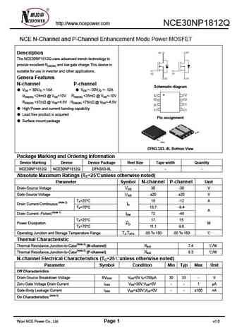
1812 MOSFET Equivalente. Reemplazo. Hoja de especificaciones. Principales características
Número de Parte: 1812
Tipo de FET: MOSFET
Polaridad de transistor: N
ESPECIFICACIONES MÁXIMAS
Pdⓘ - Máxima disipación de potencia: 41.7 W
|Vds|ⓘ - Voltaje máximo drenador-fuente: 60 V
|Vgs|ⓘ - Voltaje máximo fuente-puerta: 20 V
|Id|ⓘ - Corriente continua de drenaje: 16.9 A
Tjⓘ - Temperatura máxima de unión: 150 °C
CARACTERÍSTICAS ELÉCTRICAS
trⓘ - Tiempo de subida: 11 nS
Cossⓘ - Capacitancia de salida: 85 pF
RDSonⓘ - Resistencia estado encendido drenaje a fuente: 0.073 Ohm
Encapsulados: TO252
Búsqueda de reemplazo de 1812 MOSFET
- Selecciónⓘ de transistores por parámetros
1812 datasheet
1812.pdf
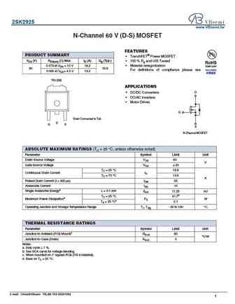
2SK2925 www.VBsemi.tw N-Channel 60 V (D-S) MOSFET FEATURES PRODUCT SUMMARY TrenchFET Power MOSFET VDS (V) RDS(on) ( ) Max. ID (A) Qg (Typ.) 100 % Rg and UIS Tested 0.073 at VGS = 10 V 18.2 Material categorization 60 19.8 For definitions of compliance please see 0.085 at VGS = 4.5 V 13.2 TO-252 APPLICATIONS D DC/DC Converters DC/AC Inverters Motor
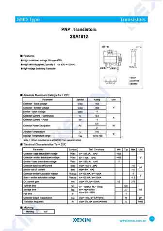
2sa1812 2sa1727 2sa1776.pdf
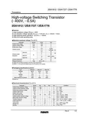
2SA1812 / 2SA1727 / 2SA1776 Transistors High-voltage Switching Transistor ( 400V, 0.5A) 2SA1812 / 2SA1727 / 2SA1776 Features 1) High breakdown voltage, BVCEO= 400V. 2) Low saturation voltage, typically VCE (sat) = 0.3V at IC / IB = 100mA / 10mA. 3) High switching speed, typically tf 1 s at IC = 100mA. 4) Wide SOA (safe operating area). Absolute maximum ratings (Ta=25 C) Paramete
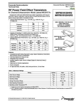
mrf7s18125ah.pdf
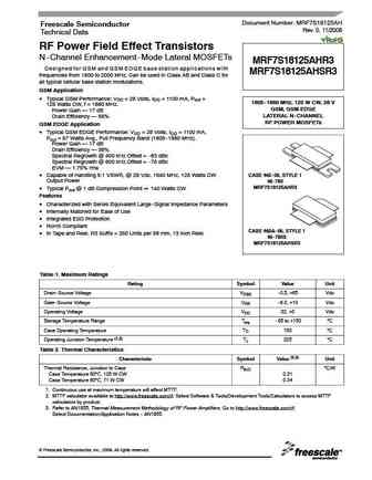
Document Number MRF7S18125AH Freescale Semiconductor Rev. 0, 11/2008 Technical Data RF Power Field Effect Transistors N-Channel Enhancement-Mode Lateral MOSFETs MRF7S18125AHR3 Designed for GSM and GSM EDGE base station applications with MRF7S18125AHSR3 frequencies from 1800 to 2000 MHz. Can be used in Class AB and Class C for all typical cellular base station modulations. GSM Applic
Otros transistores... 2SK4070D , 2SK4070I , 2SK4074LS , 2SK4075B , 2SK4081 , 2SK4081D , 13N10 , 15N10-TO251 , STP75NF75 , 1N60L-TM3-T , 20N03L-TO252 , 20N06L-TO252 , 20N3LG-TO251 , 20P06-TO252 , 25N06L-TN3 , 25NF20 , 2N0623 .
History: CS4N60A3R | ELM33408CA | VS6880AT | NCE60H10F | 2SK3288ENTL | SMP40N10 | STD3NK50Z-1
History: CS4N60A3R | ELM33408CA | VS6880AT | NCE60H10F | 2SK3288ENTL | SMP40N10 | STD3NK50Z-1
🌐 : EN ES РУ

Liste
Recientemente añadidas las descripciónes de los transistores:
MOSFET: AUB034N10 | AUB033N08BG | AUB026N085 | AUA062N08BG | AUA060N08AG | AUA056N08BGL | AUA039N10 | ASW80R290E | ASW65R120EFD | ASW65R110E | ASW65R095EFD | ASW65R046EFD | ASW65R041EFDA | ASW65R041E | ASW60R150E | ASW60R090EFDA
Popular searches
2sa1294 datasheet | mp10b transistor | bc182b | 2n3054 transistor equivalent | 2n554 | 2sa1011 | 2sa1283 | 2sb646