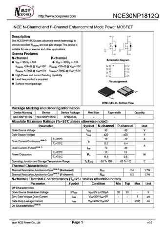
1812 Specs and Replacement
Type Designator: 1812
Type of Transistor: MOSFET
Type of Control Channel: N-Channel
Absolute Maximum Ratings
Pd ⓘ - Maximum Power Dissipation: 41.7 W
|Vds|ⓘ - Maximum Drain-Source Voltage: 60 V
|Vgs|ⓘ - Maximum Gate-Source Voltage: 20 V
|Id| ⓘ - Maximum Drain Current: 16.9 A
Tj ⓘ - Maximum Junction Temperature: 150 °C
Electrical Characteristics
tr ⓘ - Rise Time: 11 nS
Cossⓘ - Output Capacitance: 85 pF
RDSonⓘ - Maximum Drain-Source On-State Resistance: 0.073 Ohm
Package: TO252
1812 substitution
- MOSFET ⓘ Cross-Reference Search
1812 datasheet
1812.pdf
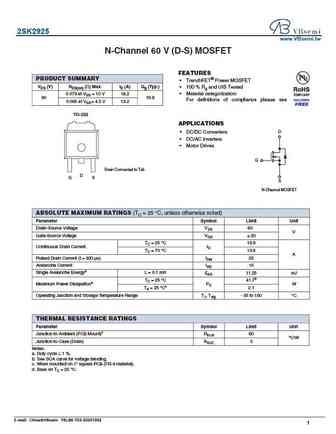
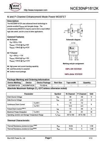
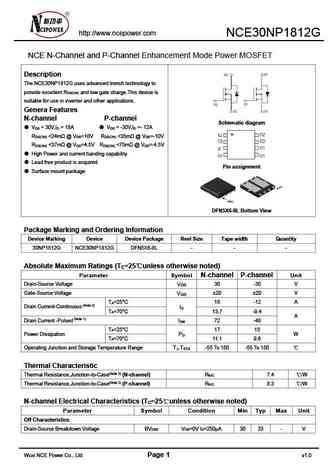
2SK2925 www.VBsemi.tw N-Channel 60 V (D-S) MOSFET FEATURES PRODUCT SUMMARY TrenchFET Power MOSFET VDS (V) RDS(on) ( ) Max. ID (A) Qg (Typ.) 100 % Rg and UIS Tested 0.073 at VGS = 10 V 18.2 Material categorization 60 19.8 For definitions of compliance please see 0.085 at VGS = 4.5 V 13.2 TO-252 APPLICATIONS D DC/DC Converters DC/AC Inverters Motor ... See More ⇒
2sa1812 2sa1727 2sa1776.pdf
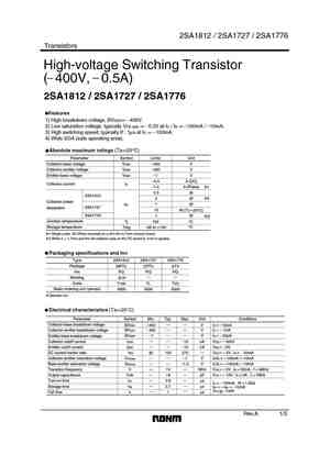
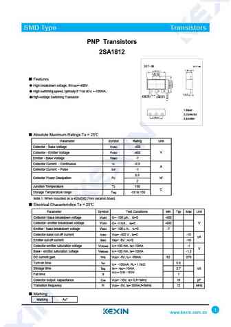
2SA1812 / 2SA1727 / 2SA1776 Transistors High-voltage Switching Transistor ( 400V, 0.5A) 2SA1812 / 2SA1727 / 2SA1776 Features 1) High breakdown voltage, BVCEO= 400V. 2) Low saturation voltage, typically VCE (sat) = 0.3V at IC / IB = 100mA / 10mA. 3) High switching speed, typically tf 1 s at IC = 100mA. 4) Wide SOA (safe operating area). Absolute maximum ratings (Ta=25 C) Paramete... See More ⇒
2sa1812.pdf
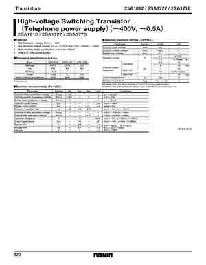
Transistors 2SA1812 / 2SA1727 / 2SA1776 (96-609-A313) 320 ... See More ⇒
mrf7s18125ah.pdf
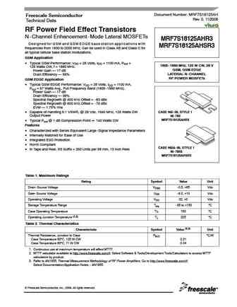
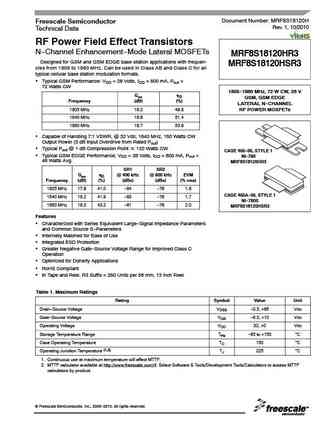
Document Number MRF7S18125AH Freescale Semiconductor Rev. 0, 11/2008 Technical Data RF Power Field Effect Transistors N-Channel Enhancement-Mode Lateral MOSFETs MRF7S18125AHR3 Designed for GSM and GSM EDGE base station applications with MRF7S18125AHSR3 frequencies from 1800 to 2000 MHz. Can be used in Class AB and Class C for all typical cellular base station modulations. GSM Applic... See More ⇒
Detailed specifications: 2SK4070D, 2SK4070I, 2SK4074LS, 2SK4075B, 2SK4081, 2SK4081D, 13N10, 15N10-TO251, STP75NF75, 1N60L-TM3-T, 20N03L-TO252, 20N06L-TO252, 20N3LG-TO251, 20P06-TO252, 25N06L-TN3, 25NF20, 2N0623
Keywords - 1812 MOSFET specs
1812 cross reference
1812 equivalent finder
1812 pdf lookup
1812 substitution
1812 replacement
Step-by-step guide to finding a MOSFET replacement. Cross-reference parts and ensure compatibility for your repair or project.
History: 2SK3681 | STK1820F
🌐 : EN ES РУ
LIST
Last Update
MOSFET: AUB034N10 | AUB033N08BG | AUB026N085 | AUA062N08BG | AUA060N08AG | AUA056N08BGL | AUA039N10 | ASW80R290E | ASW65R120EFD | ASW65R110E
Popular searches
2sa1294 datasheet | mp10b transistor | bc182b | 2n3054 transistor equivalent | 2n554 | 2sa1011 | 2sa1283 | 2sb646
