1812. Аналоги и основные параметры
Наименование производителя: 1812
Тип транзистора: MOSFET
Полярность: N
Предельные значения
Pd ⓘ - Максимальная рассеиваемая мощность: 41.7 W
|Vds|ⓘ - Максимально допустимое напряжение сток-исток: 60 V
|Vgs|ⓘ - Максимально допустимое напряжение затвор-исток: 20 V
|Id| ⓘ - Максимально допустимый постоянный ток стока: 16.9 A
Tj ⓘ - Максимальная температура канала: 150 °C
Электрические характеристики
tr ⓘ - Время нарастания: 11 ns
Cossⓘ - Выходная емкость: 85 pf
RDSonⓘ - Сопротивление сток-исток открытого транзистора: 0.073 Ohm
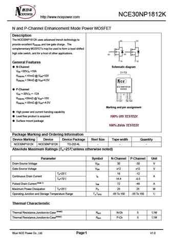
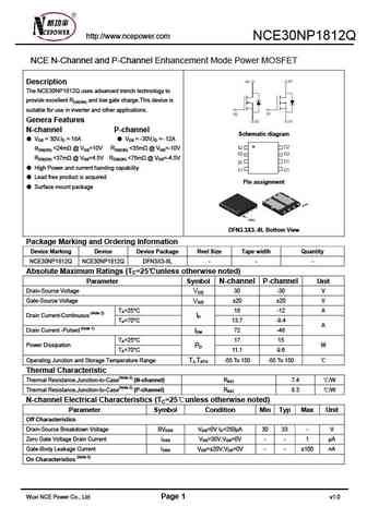
Тип корпуса: TO252
Аналог (замена) для 1812
- подборⓘ MOSFET транзистора по параметрам
1812 даташит
1812.pdf
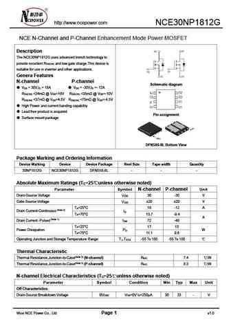
2SK2925 www.VBsemi.tw N-Channel 60 V (D-S) MOSFET FEATURES PRODUCT SUMMARY TrenchFET Power MOSFET VDS (V) RDS(on) ( ) Max. ID (A) Qg (Typ.) 100 % Rg and UIS Tested 0.073 at VGS = 10 V 18.2 Material categorization 60 19.8 For definitions of compliance please see 0.085 at VGS = 4.5 V 13.2 TO-252 APPLICATIONS D DC/DC Converters DC/AC Inverters Motor
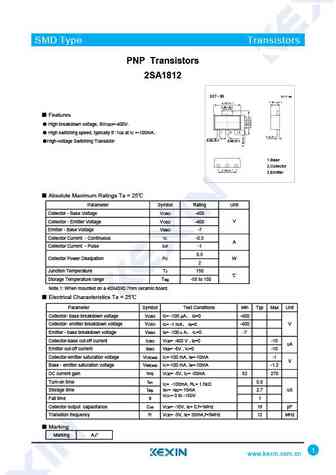
2sa1812 2sa1727 2sa1776.pdf
2SA1812 / 2SA1727 / 2SA1776 Transistors High-voltage Switching Transistor ( 400V, 0.5A) 2SA1812 / 2SA1727 / 2SA1776 Features 1) High breakdown voltage, BVCEO= 400V. 2) Low saturation voltage, typically VCE (sat) = 0.3V at IC / IB = 100mA / 10mA. 3) High switching speed, typically tf 1 s at IC = 100mA. 4) Wide SOA (safe operating area). Absolute maximum ratings (Ta=25 C) Paramete
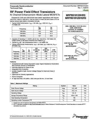
mrf7s18125ah.pdf
Document Number MRF7S18125AH Freescale Semiconductor Rev. 0, 11/2008 Technical Data RF Power Field Effect Transistors N-Channel Enhancement-Mode Lateral MOSFETs MRF7S18125AHR3 Designed for GSM and GSM EDGE base station applications with MRF7S18125AHSR3 frequencies from 1800 to 2000 MHz. Can be used in Class AB and Class C for all typical cellular base station modulations. GSM Applic
Другие MOSFET... 2SK4070D , 2SK4070I , 2SK4074LS , 2SK4075B , 2SK4081 , 2SK4081D , 13N10 , 15N10-TO251 , STP75NF75 , 1N60L-TM3-T , 20N03L-TO252 , 20N06L-TO252 , 20N3LG-TO251 , 20P06-TO252 , 25N06L-TN3 , 25NF20 , 2N0623 .
History: 2SK293 | SMK0825FC | SM6012NSUB
History: 2SK293 | SMK0825FC | SM6012NSUB
🌐 : EN ES РУ

Список транзисторов
Обновления
MOSFET: ASU70R600E | ASU65R850E | ASU65R550E | ASU65R350E | ASR65R120EFD | ASR65R046EFD | ASQ65R046EFD | ASM65R280E | ASM60R330E | ASE70R950E | ASD80R750E | ASD70R950E | ASD70R600E | ASD70R380E | ASD65R850E | ASD65R550E
Popular searches
2sa1294 datasheet | mp10b transistor | bc182b | 2n3054 transistor equivalent | 2n554 | 2sa1011 | 2sa1283 | 2sb646