FDN335N-NL MOSFET Equivalente. Reemplazo. Hoja de especificaciones. Principales características
Número de Parte: FDN335N-NL
Tipo de FET: MOSFET
Polaridad de transistor: N
ESPECIFICACIONES MÁXIMAS
Pdⓘ - Máxima disipación de potencia: 1.25 W
|Vds|ⓘ - Voltaje máximo drenador-fuente: 20 V
|Vgs|ⓘ - Voltaje máximo fuente-puerta: 12 V
|Id|ⓘ - Corriente continua de drenaje: 5 A
Tjⓘ - Temperatura máxima de unión: 150 °C
CARACTERÍSTICAS ELÉCTRICAS
trⓘ - Tiempo de subida: 17 nS
Cossⓘ - Capacitancia de salida: 105 pF
RDSonⓘ - Resistencia estado encendido drenaje a fuente: 0.028 typ Ohm
Encapsulados: SOT23
Búsqueda de reemplazo de FDN335N-NL MOSFET
- Selecciónⓘ de transistores por parámetros
FDN335N-NL datasheet
fdn335n-nl.pdf
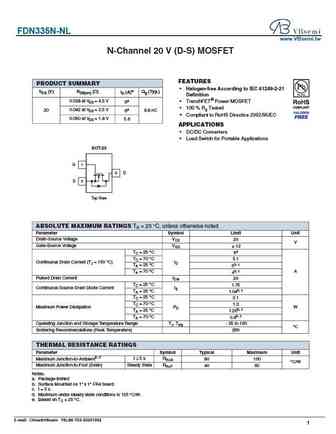
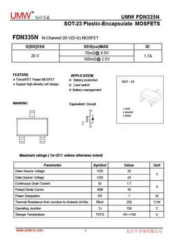
FDN335N-NL www.VBsemi.tw N-Channel 20 V (D-S) MOSFET FEATURES PRODUCT SUMMARY Halogen-free According to IEC 61249-2-21 VDS (V) RDS(on) ( ) ID (A)e Qg (Typ.) Definition 0.028 at VGS = 4.5 V TrenchFET Power MOSFET 6a 100 % Rg Tested 20 0.042 at VGS = 2.5 V 6a 8.8 nC Compliant to RoHS Directive 2002/95/EC 0.050 at VGS = 1.8 V 5.6 APPLICATIONS DC/D
fdn335n.pdf
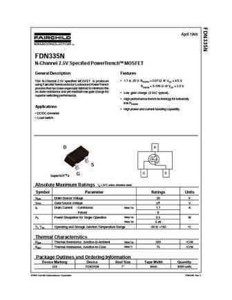
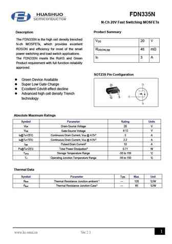
April 1999 FDN335N N-Channel 2.5V Specified PowerTrenchTM MOSFET General Description Features 1.7 A, 20 V. RDS(ON) = 0.07 @ VGS = 4.5 V This N-Channel 2.5V specified MOSFET is produced using Fairchild Semiconductor's advanced PowerTrench RDS(ON) = 0.100 @ VGS = 2.5 V. process that has been especially tailored to minimize the on-state resistance and yet maintain low gate cha
fdn335n.pdf
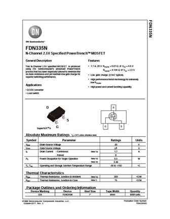
FDN335N N-Channel 2.5V Specified PowerTrenchTM MOSFET General Description Features 1.7 A, 20 V. RDS(ON) = 0.07 @ VGS = 4.5 V This N-Channel 2.5V specified MOSFET is produced using ON Semiconductor's advanced PowerTrench RDS(ON) = 0.100 @ VGS = 2.5 V. process that has been especially tailored to minimize the on-state resistance and yet maintain low gate charge for Lo
fdn335n.pdf
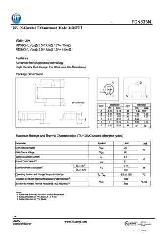
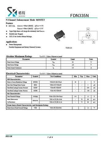
FDN335N 20V N-Channel Enhancement Mode MOSFET VDS= 20V RDS(ON), Vgs@ 2.5V, Ids@ 1.7A= 70m RDS(ON), Vgs@ 2.5V, Ids@ 1.5A= 100m Features Advanced trench process technology High Density Cell Design For Ultra Low On-Resistance Package Dimensions D G S SOT-23(PACKAGE) Millimeter Millimeter REF. REF. Min. Max. Min. Max. A 2.70 3.10 G 1.90 REF. B 2.40 2.80 H 1.00
Otros transistores... EMB60N06A , EMFA0P02J , F3055L-TO252 , FDD390N15AL , FDD3N40TM , FDD8444-NL , FDD8580-6 , FDN304P-NL , 75N75 , FDN337N-NL , FDN338P-NL , FDS4435-NL , FDS4450 , FDS4465-NL-9 , FDS4685-NL , FDS4897A , FDS4935BZ-NL-38 .
🌐 : EN ES РУ

Liste
Recientemente añadidas las descripciónes de los transistores:
MOSFET: AUB062N08BG | AUB060N08AG | AUB056N10 | AUB056N08BGL | AUB050N085 | AUB050N055 | AUB045N12 | AUB045N10BT | AUB039N10 | AUB034N10 | AUB033N08BG | AUB026N085 | AUA062N08BG | AUA060N08AG | AUA056N08BGL | AUA039N10
Popular searches
irf9540n | bd139 datasheet | irf9640 | 2n3053 | a1015 | mpsa42 | 2n5551 transistor | a1015 transistor