FDN335N-NL Specs and Replacement
Type Designator: FDN335N-NL
Type of Transistor: MOSFET
Type of Control Channel: N-Channel
Absolute Maximum Ratings
Pd ⓘ - Maximum Power Dissipation: 1.25 W
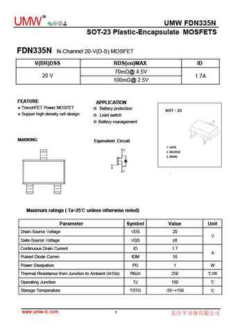
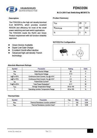
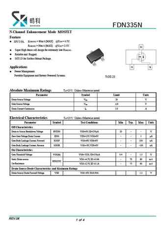
|Vds|ⓘ - Maximum Drain-Source Voltage: 20 V
|Vgs|ⓘ - Maximum Gate-Source Voltage: 12 V
|Id| ⓘ - Maximum Drain Current: 5 A
Tj ⓘ - Maximum Junction Temperature: 150 °C
Electrical Characteristics
tr ⓘ - Rise Time: 17 nS
Cossⓘ - Output Capacitance: 105 pF
RDSonⓘ - Maximum Drain-Source On-State Resistance: 0.028 typ Ohm
Package: SOT23
FDN335N-NL substitution
- MOSFET ⓘ Cross-Reference Search
FDN335N-NL datasheet
fdn335n-nl.pdf
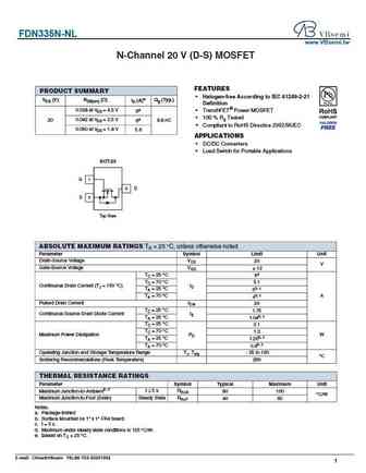
FDN335N-NL www.VBsemi.tw N-Channel 20 V (D-S) MOSFET FEATURES PRODUCT SUMMARY Halogen-free According to IEC 61249-2-21 VDS (V) RDS(on) ( ) ID (A)e Qg (Typ.) Definition 0.028 at VGS = 4.5 V TrenchFET Power MOSFET 6a 100 % Rg Tested 20 0.042 at VGS = 2.5 V 6a 8.8 nC Compliant to RoHS Directive 2002/95/EC 0.050 at VGS = 1.8 V 5.6 APPLICATIONS DC/D... See More ⇒
fdn335n.pdf
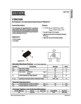
April 1999 FDN335N N-Channel 2.5V Specified PowerTrenchTM MOSFET General Description Features 1.7 A, 20 V. RDS(ON) = 0.07 @ VGS = 4.5 V This N-Channel 2.5V specified MOSFET is produced using Fairchild Semiconductor's advanced PowerTrench RDS(ON) = 0.100 @ VGS = 2.5 V. process that has been especially tailored to minimize the on-state resistance and yet maintain low gate cha... See More ⇒
fdn335n.pdf
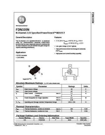
FDN335N N-Channel 2.5V Specified PowerTrenchTM MOSFET General Description Features 1.7 A, 20 V. RDS(ON) = 0.07 @ VGS = 4.5 V This N-Channel 2.5V specified MOSFET is produced using ON Semiconductor's advanced PowerTrench RDS(ON) = 0.100 @ VGS = 2.5 V. process that has been especially tailored to minimize the on-state resistance and yet maintain low gate charge for Lo... See More ⇒
fdn335n.pdf
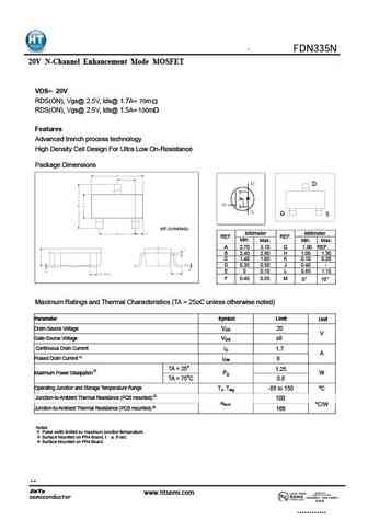
FDN335N 20V N-Channel Enhancement Mode MOSFET VDS= 20V RDS(ON), Vgs@ 2.5V, Ids@ 1.7A= 70m RDS(ON), Vgs@ 2.5V, Ids@ 1.5A= 100m Features Advanced trench process technology High Density Cell Design For Ultra Low On-Resistance Package Dimensions D G S SOT-23(PACKAGE) Millimeter Millimeter REF. REF. Min. Max. Min. Max. A 2.70 3.10 G 1.90 REF. B 2.40 2.80 H 1.00... See More ⇒
Detailed specifications: EMB60N06A, EMFA0P02J, F3055L-TO252, FDD390N15AL, FDD3N40TM, FDD8444-NL, FDD8580-6, FDN304P-NL, 75N75, FDN337N-NL, FDN338P-NL, FDS4435-NL, FDS4450, FDS4465-NL-9, FDS4685-NL, FDS4897A, FDS4935BZ-NL-38
Keywords - FDN335N-NL MOSFET specs
FDN335N-NL cross reference
FDN335N-NL equivalent finder
FDN335N-NL pdf lookup
FDN335N-NL substitution
FDN335N-NL replacement
Need a MOSFET replacement? Our guide shows you how to find a perfect substitute by comparing key parameters and specs
🌐 : EN ES РУ

LIST
Last Update
MOSFET: AUB034N10 | AUB033N08BG | AUB026N085 | AUA062N08BG | AUA060N08AG | AUA056N08BGL | AUA039N10 | ASW80R290E | ASW65R120EFD | ASW65R110E
Popular searches
irf9540n | bd139 datasheet | irf9640 | 2n3053 | a1015 | mpsa42 | 2n5551 transistor | a1015 transistor