FDC6320C MOSFET Equivalente. Reemplazo. Hoja de especificaciones. Principales características
Número de Parte: FDC6320C
Tipo de FET: MOSFET
Polaridad de transistor: NP
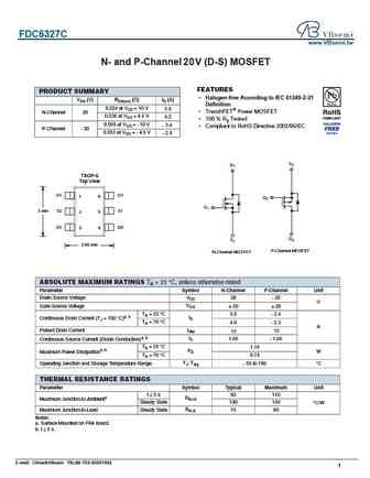
ESPECIFICACIONES MÁXIMAS
Pdⓘ - Máxima disipación de potencia: 0.9 W|Vds|ⓘ - Voltaje máximo drenador - fuente: 25 V
|Vgs|ⓘ - Voltaje máximo fuente - puerta: 8 V
|Id|ⓘ - Corriente continua de drenaje: 0.22(0.12) A
Tjⓘ - Temperatura máxima de unión: 150 °C
CARACTERÍSTICAS ELÉCTRICAS
trⓘ - Tiempo de subida: 4.5(6) nS
Cossⓘ - Capacitancia de salida: 6(7) pF
Rds(on)ⓘ - Resistencia estado encendido drenaje a fuente: 5(13) Ohm
Paquete / Cubierta: SSOT6
Búsqueda de reemplazo de FDC6320C MOSFET
FDC6320C datasheet
fdc6320c.pdf
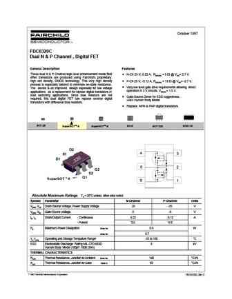
October 1997 FDC6320C Dual N & P Channel , Digital FET General Description Features These dual N & P Channel logic level enhancement mode field N-Ch 25 V, 0.22 A, RDS(ON) = 5 @ VGS= 2.7 V. effec transistors are produced using Fairchild's proprietary, high cell density, DMOS technology. This very high density P-Ch 25 V, -0.12 A, RDS(ON) = 13 @ VGS= -2.7 V. process is especial
fdc6323l.pdf
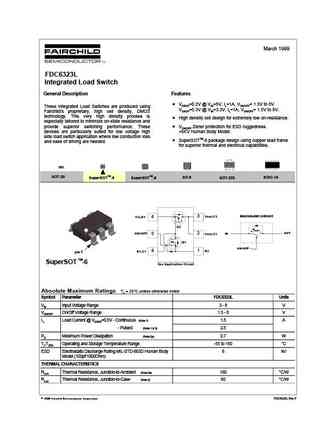
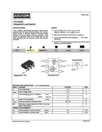
March 1999 FDC6323L Integrated Load Switch General Description Features VDROP=0.2V @ VIN=5V, IL=1A, VON/OFF= 1.5V to 8V These Integrated Load Switches are produced using VDROP=0.3V @ VIN=3.3V, IL=1A, VON/OFF= 1.5V to 8V. Fairchild's proprietary, high cell density, DMOS technology. This very high density process is High density cell design for extremely low on-resistance. especially
fdc6321c.pdf
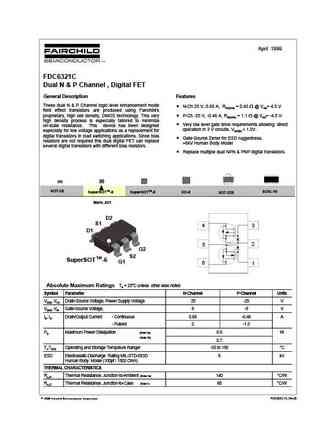
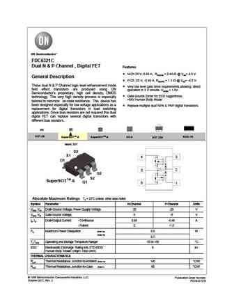
April 1999 FDC6321C Dual N & P Channel , Digital FET General Description Features These dual N & P Channel logic level enhancement mode N-Ch 25 V, 0.68 A, RDS(ON) = 0.45 @ VGS= 4.5 V field effect transistors are produced using Fairchild's proprietary, high cell density, DMOS technology. This very P-Ch -25 V, -0.46 A, RDS(ON) = 1.1 @ VGS= -4.5 V. high density process is especi
fdc6329l.pdf
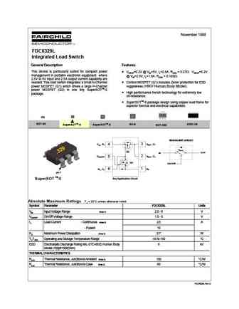
November 1998 FDC6329L Integrated Load Switch General Description Features This device is particularly suited for compact power VDROP=0.2V @ VIN=5V, IL=2.8A. R(ON) = 0.07 VDROP=0.2V management in portable electronic equipment where @ VIN=2.5V, IL=1.9A. R(ON) = 0.105 . 2.5V to 8V input and 2.5A output current capability are needed. This load switch integrates a small N-Channel

Otros transistores... FDC602P , FDC604P , FDC606P , FDC608PZ , FDC610PZ , FDC6310P , FDC6312P , FDC6318P , IRF640N , STU303S , FDC6321C , STU3030NLS , FDC6327C , STU17L01 , FDC6333C , STU16L01 , STU15N20 .
History: FDC6310P
History: FDC6310P
🌐 : EN ES РУ

Liste
Recientemente añadidas las descripciónes de los transistores:
MOSFET: HAF1008S | HAF1008L | EMZB08P03H | CS30N20FA9R | AOT66613L | AOSP21313C | AOSP21311C | AOB66918L | AO3415C | AOTF20N40L | AOTF11N60L | AOT11N60L | AONS21303C | AOI280A60 | AOB66914L | AO3485C
Popular searches
mj15024 | 2n2219 | tip42c | 2sc2240 | bc547 transistor equivalent | 2sa1943 | tip41c datasheet | mje15032