FDC6327C MOSFET Equivalente. Reemplazo. Hoja de especificaciones. Principales características
Número de Parte: FDC6327C
Tipo de FET: MOSFET
Polaridad de transistor: NP
ESPECIFICACIONES MÁXIMAS
Pdⓘ - Máxima disipación de potencia: 0.96 W|Vds|ⓘ - Voltaje máximo drenador - fuente: 20 V
|Vgs|ⓘ - Voltaje máximo fuente - puerta: 8 V
|Id|ⓘ - Corriente continua de drenaje: 2.7(1.6) A
Tjⓘ - Temperatura máxima de unión: 150 °C
CARACTERÍSTICAS ELÉCTRICAS
trⓘ - Tiempo de subida: 9(14) nS
Cossⓘ - Capacitancia de salida: 75(65) pF
Rds(on)ⓘ - Resistencia estado encendido drenaje a fuente: 0.08(0.17) Ohm
Paquete / Cubierta: SSOT6
Búsqueda de reemplazo de FDC6327C MOSFET
FDC6327C datasheet
fdc6327c.pdf
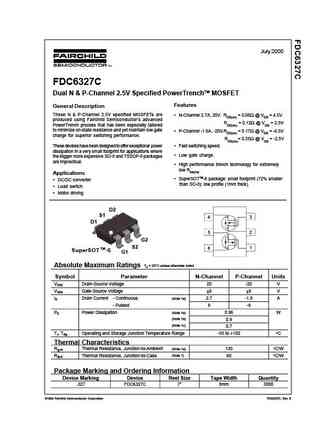
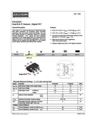
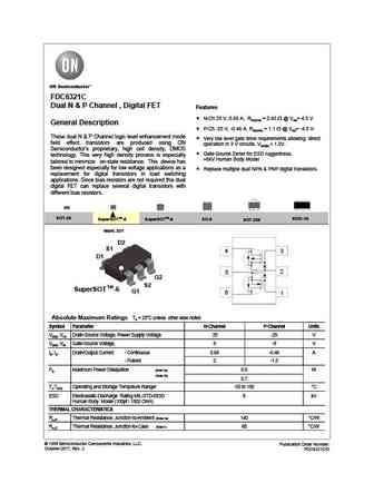
July 2000 FDC6327C Dual N & P-Channel 2.5V Specified PowerTrenchTM MOSFET Features General Description These N & P-Channel 2.5V specified MOSFETs are N-Channel 2.7A, 20V. RDS(on) = 0.08 @ VGS = 4.5V produced using Fairchild Semiconductor's advanced RDS(on) = 0.12 @ VGS = 2.5V PowerTrench process that has been especially tailored to minimize on-state resistance and yet mainta
fdc6327c.pdf

Is Now Part of To learn more about ON Semiconductor, please visit our website at www.onsemi.com ON Semiconductor and the ON Semiconductor logo are trademarks of Semiconductor Components Industries, LLC dba ON Semiconductor or its subsidiaries in the United States and/or other countries. ON Semiconductor owns the rights to a number of patents, trademarks, copyrights, trade secrets, and oth
fdc6327c.pdf
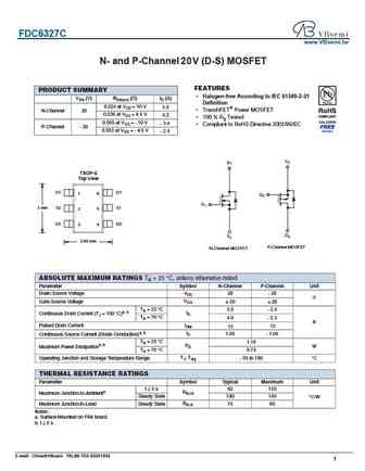
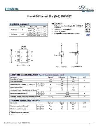
FDC6327C www.VBsemi.tw N- and P-Channel 2 V (D-S) MOSFET 0 FEATURES PRODUCT SUMMARY Halogen-free According to IEC 61249-2-21 VDS (V) RDS(on) ( )ID (A) Definition 0.024 at VGS = 10 V 5.5 TrenchFET Power MOSFET N-Channel 20 0.036 at VGS = 4.5 V 4.2 100 % Rg Tested 0.069 at VGS = - 10 V - 3.4 Compliant to RoHS Directive 2002/95/EC P-Channel - 20 0.083 at V
fdc6323l.pdf
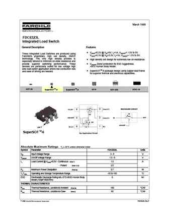
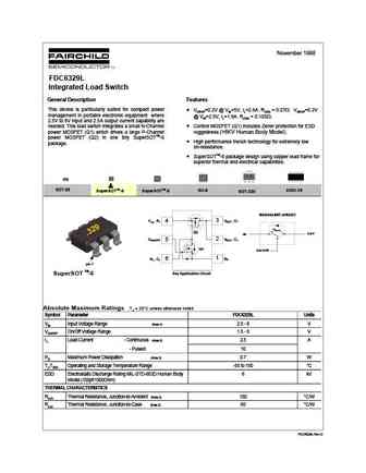
March 1999 FDC6323L Integrated Load Switch General Description Features VDROP=0.2V @ VIN=5V, IL=1A, VON/OFF= 1.5V to 8V These Integrated Load Switches are produced using VDROP=0.3V @ VIN=3.3V, IL=1A, VON/OFF= 1.5V to 8V. Fairchild's proprietary, high cell density, DMOS technology. This very high density process is High density cell design for extremely low on-resistance. especially
Otros transistores... FDC610PZ , FDC6310P , FDC6312P , FDC6318P , FDC6320C , STU303S , FDC6321C , STU3030NLS , IRF3710 , STU17L01 , FDC6333C , STU16L01 , STU15N20 , FDC637BNZ , FDC638APZ , FDC6401N , FDC6420C .
🌐 : EN ES РУ

Liste
Recientemente añadidas las descripciónes de los transistores:
MOSFET: HAF1008S | HAF1008L | EMZB08P03H | CS30N20FA9R | AOT66613L | AOSP21313C | AOSP21311C | AOB66918L | AO3415C | AOTF20N40L | AOTF11N60L | AOT11N60L | AONS21303C | AOI280A60 | AOB66914L | AO3485C
Popular searches
bc547 transistor equivalent | 2sa1943 | tip41c datasheet | mje15032 | tip32c datasheet | mje15032g | irf1404 | bc550