FDC6327C Specs and Replacement
Type Designator: FDC6327C
Type of Transistor: MOSFET
Type of Control Channel: NP-Channel
Absolute Maximum Ratings
Pd ⓘ - Maximum Power Dissipation: 0.96 W
|Vds|ⓘ - Maximum Drain-Source Voltage: 20 V
|Vgs|ⓘ - Maximum Gate-Source Voltage: 8 V
|Id| ⓘ - Maximum Drain Current: 2.7(1.6) A
Tj ⓘ - Maximum Junction Temperature: 150 °C
Electrical Characteristics
tr ⓘ - Rise Time: 9(14) nS
Cossⓘ - Output Capacitance: 75(65) pF
Rds ⓘ - Maximum Drain-Source On-State Resistance: 0.08(0.17) Ohm
Package: SSOT6
FDC6327C substitution
- MOSFET ⓘ Cross-Reference Search
FDC6327C datasheet
fdc6327c.pdf
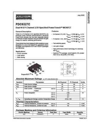
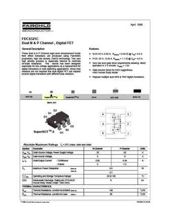
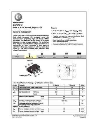
July 2000 FDC6327C Dual N & P-Channel 2.5V Specified PowerTrenchTM MOSFET Features General Description These N & P-Channel 2.5V specified MOSFETs are N-Channel 2.7A, 20V. RDS(on) = 0.08 @ VGS = 4.5V produced using Fairchild Semiconductor's advanced RDS(on) = 0.12 @ VGS = 2.5V PowerTrench process that has been especially tailored to minimize on-state resistance and yet mainta... See More ⇒
fdc6327c.pdf

Is Now Part of To learn more about ON Semiconductor, please visit our website at www.onsemi.com ON Semiconductor and the ON Semiconductor logo are trademarks of Semiconductor Components Industries, LLC dba ON Semiconductor or its subsidiaries in the United States and/or other countries. ON Semiconductor owns the rights to a number of patents, trademarks, copyrights, trade secrets, and oth... See More ⇒
fdc6327c.pdf
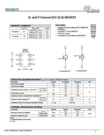
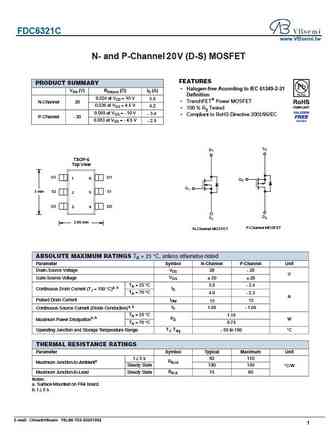
FDC6327C www.VBsemi.tw N- and P-Channel 2 V (D-S) MOSFET 0 FEATURES PRODUCT SUMMARY Halogen-free According to IEC 61249-2-21 VDS (V) RDS(on) ( )ID (A) Definition 0.024 at VGS = 10 V 5.5 TrenchFET Power MOSFET N-Channel 20 0.036 at VGS = 4.5 V 4.2 100 % Rg Tested 0.069 at VGS = - 10 V - 3.4 Compliant to RoHS Directive 2002/95/EC P-Channel - 20 0.083 at V... See More ⇒
fdc6323l.pdf
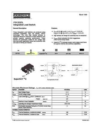
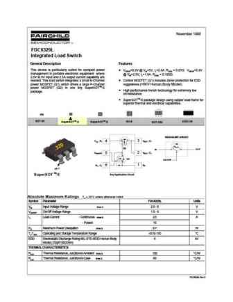
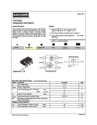
March 1999 FDC6323L Integrated Load Switch General Description Features VDROP=0.2V @ VIN=5V, IL=1A, VON/OFF= 1.5V to 8V These Integrated Load Switches are produced using VDROP=0.3V @ VIN=3.3V, IL=1A, VON/OFF= 1.5V to 8V. Fairchild's proprietary, high cell density, DMOS technology. This very high density process is High density cell design for extremely low on-resistance. especially... See More ⇒
Detailed specifications: FDC610PZ , FDC6310P , FDC6312P , FDC6318P , FDC6320C , STU303S , FDC6321C , STU3030NLS , IRF3710 , STU17L01 , FDC6333C , STU16L01 , STU15N20 , FDC637BNZ , FDC638APZ , FDC6401N , FDC6420C .
History: STU3030NLS | 2SK3467 | IRF2907ZS-7PPBF | APA2N70K-HF
Keywords - FDC6327C MOSFET specs
FDC6327C cross reference
FDC6327C equivalent finder
FDC6327C pdf lookup
FDC6327C substitution
FDC6327C replacement
Can't find your MOSFET? Learn how to find a substitute transistor by analyzing voltage, current and package compatibility
History: STU3030NLS | 2SK3467 | IRF2907ZS-7PPBF | APA2N70K-HF
🌐 : EN ES РУ

LIST
Last Update
MOSFET: HAF1008S | HAF1008L | EMZB08P03H | CS30N20FA9R | AOT66613L | AOSP21313C | AOSP21311C | AOB66918L | AO3415C | AOTF20N40L
Popular searches
bc547 transistor equivalent | 2sa1943 | tip41c datasheet | mje15032 | tip32c datasheet | mje15032g | irf1404 | bc550