FDG6321C Datasheet. Equivalente. Reemplazo. Hoja de especificaciones. Principales características
Número de Parte: FDG6321C 📄📄
Tipo de FET: MOSFET
Polaridad de transistor: NP
ESPECIFICACIONES MÁXIMAS
Pdⓘ - Máxima disipación de potencia: 0.3 W
|Vds|ⓘ - Voltaje máximo drenador-fuente: 25 V
|Vgs|ⓘ - Voltaje máximo fuente-puerta: 8 V
|Id|ⓘ - Corriente continua de drenaje: 0.5 A
Tjⓘ - Temperatura máxima de unión: 150 °C
CARACTERÍSTICAS ELÉCTRICAS
RDSonⓘ - Resistencia estado encendido drenaje a fuente: 0.45 Ohm
Encapsulados: SC70
📄📄 Copiar
Búsqueda de reemplazo de FDG6321C MOSFET
- Selecciónⓘ de transistores por parámetros
FDG6321C datasheet
fdg6321c.pdf
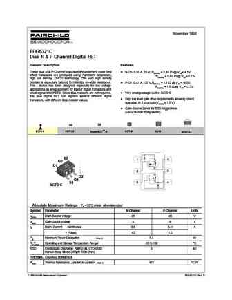
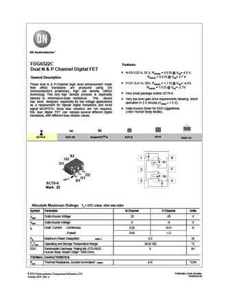
November 1998 FDG6321C Dual N & P Channel Digital FET General Description Features These dual N & P-Channel logic level enhancement mode field N-Ch 0.50 A, 25 V, RDS(ON) = 0.45 @ VGS= 4.5V. effect transistors are produced using Fairchild's proprietary, RDS(ON) = 0.60 @ VGS= 2.7 V. high cell density, DMOS technology. This very high density process is especially tailored to mi
fdg6321c.pdf
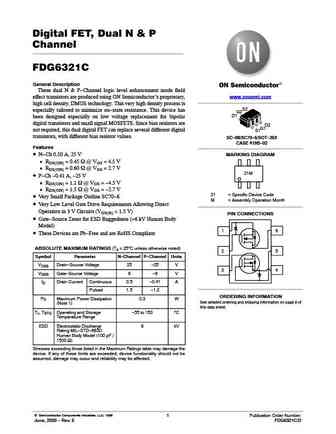
Digital FET, Dual N & P Channel FDG6321C General Description These dual N & P-Channel logic level enhancement mode field www.onsemi.com effect transistors are produced using ON Semiconductor s proprietary, high cell density, DMOS technology. This very high density process is S2 especially tailored to minimize on-state resistance. This device has G2 D1 been designed especially on l
fdg6322c.pdf
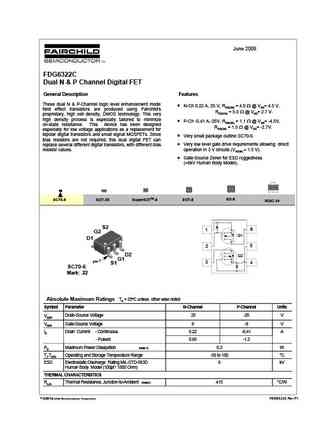
June 2008 FDG6322C Dual N & P Channel Digital FET General Description Features These dual N & P-Channel logic level enhancement mode N-Ch 0.22 A, 25 V, RDS(ON) = 4.0 @ VGS= 4.5 V, field effect transistors are produced using Fairchild's RDS(ON) = 5.0 @ VGS= 2.7 V. proprietary, high cell density, DMOS technology. This very high density process is especially tailored to minimiz
fdg6320c.pdf
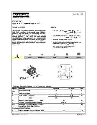
November 1998 FDG6320C Dual N & P Channel Digital FET General Description Features These dual N & P-Channel logic level enhancement mode N-Ch 0.22 A, 25 V, RDS(ON) = 4.0 @ VGS= 4.5 V, field effect transistors are produced using Fairchild's RDS(ON) = 5.0 @ VGS= 2.7 V. proprietary, high cell density, DMOS technology. This very high density process is especially tailored to mi
Otros transistores... FDG6306P, FDG6308P, FDG6316P, FDG6317NZ, FDG6318P, FDG6318PZ, FDG6320C, STS4501, IRFB31N20D, STS4300, FDG6322C, STS400, FDG6332C, STS3623, FDG6332CF085, STS3621, FDG6335N
Parámetros del MOSFET. Cómo se afectan entre sí.
History: FDD8796
🌐 : EN ES РУ

Liste
Recientemente añadidas las descripciónes de los transistores:
MOSFET: CEZC2P07 | CEZ2R05 | CEU3133 | CES2361 | CES2312A | CEP100N10L | CEM3425 | CEM3139 | CEM3133 | CEM3115 | CED3133 | CEC3257 | CEC2533 | CEB100N10L | BC3134KT | BC3134K
Popular searches
2sc1775 | 2n1305 | 2sc5242 | irf540 equivalent | mp1620 transistor equivalent | 2sc945 transistor | c2073 transistor | ac176 transistor