MEE3712H MOSFET Equivalente. Reemplazo. Hoja de especificaciones. Principales características
Número de Parte: MEE3712H
Tipo de FET: MOSFET
Polaridad de transistor: N
ESPECIFICACIONES MÁXIMAS
Pdⓘ - Máxima disipación de potencia: 125 W
|Vds|ⓘ - Voltaje máximo drenador-fuente: 100 V
|Vgs|ⓘ - Voltaje máximo fuente-puerta: 20 V
|Id|ⓘ - Corriente continua de drenaje: 57.5 A
Tjⓘ - Temperatura máxima de unión: 150 °C
CARACTERÍSTICAS ELÉCTRICAS
trⓘ - Tiempo de subida: 21 nS
Cossⓘ - Capacitancia de salida: 572 pF
RDSonⓘ - Resistencia estado encendido drenaje a fuente: 0.018 Ohm
Encapsulados: TO263
Búsqueda de reemplazo de MEE3712H MOSFET
- Selecciónⓘ de transistores por parámetros
MEE3712H datasheet
mee3712h.pdf
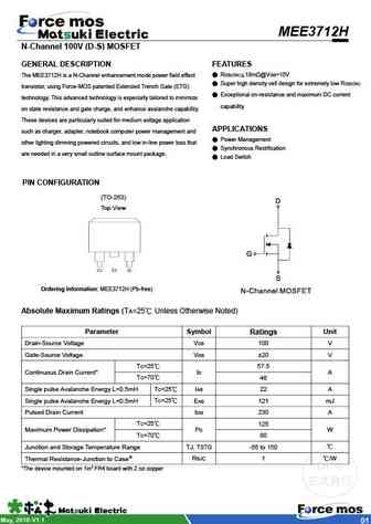
MEE3712H N-Channel 100V (D-S) MOSFET GENERAL DESCRIPTION FEATURES RDS(ON) 18m @VGS=10V The MEE3712H is a N-Channel enhancement mode power field effect Super high density cell design for extremely low RDS(ON) transistor, using Force-MOS patented Extended Trench Gate (ETG) Exceptional on-resistance and maximum DC current technology. This advanced technology is espec
mee3712t.pdf

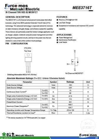
MEE3712T N-Channel 100V (D-S) MOSFET GENERAL DESCRIPTION FEATURES RDS(ON) 18m @VGS=10V The MEE3712T is a N-Channel enhancement mode power field effect Super high density cell design for extremely low RDS(ON) transistor, using Force-MOS patented Extended Trench Gate (ETG) Exceptional on-resistance and maximum DC current technology. This advanced technology is espec
mee3712f.pdf
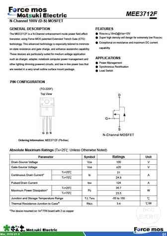
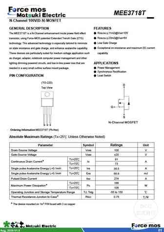
MEE3712F N-Channel 100V (D-S) MOSFET GENERAL DESCRIPTION FEATURES RDS(ON) 18m @VGS=10V The MEE3712F is a N-Channel enhancement mode power field effect Super high density cell design for extremely low RDS(ON) transistor, using Force-MOS patented Extended Trench Gate (ETG) Exceptional on-resistance and maximum DC current technology. This advanced technology is espec
mee3710t.pdf
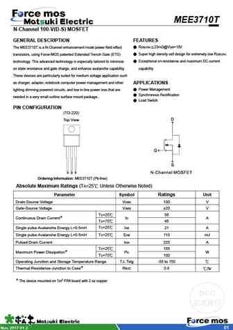
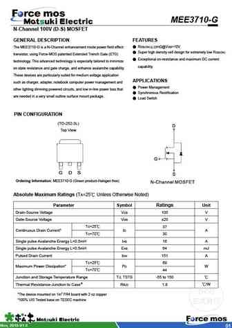
MEE3710T N-Channel 100-V(D-S) MOSFET GENERAL DESCRIPTION FEATURES The MEE3710T is a N-Channel enhancement mode power field effect RDS(ON) 23m @VGS=10V transistors, using Force-MOS patented Extended Trench Gate (ETG) Super high density cell design for extremely low RDS(ON) technology. This advanced technology is especially tailored to minimize Exceptional on-resistance
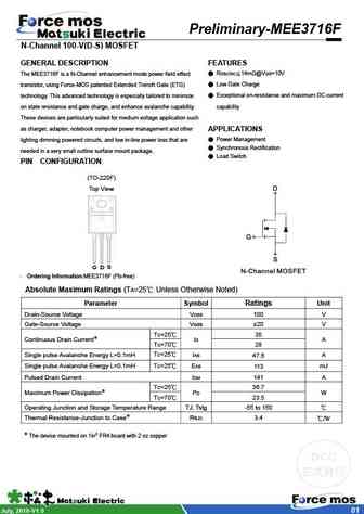
Otros transistores... ME9435AS-G , ME95N10F , ME95N10F-G , ME96N03-G , MEE2348 , MEE2348-G , MEE3710T , MEE3712F , IRFB4227 , MEE3712T , MEE3716F , MEE3716T , MEE3718T , MEE4292-G , MEE4292HP-G , MEE4292HT , MEE4292K-G .
History: CRST045N10N | MEE2348-G | SMG2328NE
History: CRST045N10N | MEE2348-G | SMG2328NE
🌐 : EN ES РУ

Liste
Recientemente añadidas las descripciónes de los transistores:
MOSFET: AUB062N08BG | AUB060N08AG | AUB056N10 | AUB056N08BGL | AUB050N085 | AUB050N055 | AUB045N12 | AUB045N10BT | AUB039N10 | AUB034N10 | AUB033N08BG | AUB026N085 | AUA062N08BG | AUA060N08AG | AUA056N08BGL | AUA039N10
Popular searches
2sc1345 | 2sd555 | a950 transistor | k2611 | c1740 transistor | c828 transistor | c4467 | c2383 transistor