NCE20P05Y MOSFET Equivalente. Reemplazo. Hoja de especificaciones. Principales características
Número de Parte: NCE20P05Y
Tipo de FET: MOSFET
Polaridad de transistor: P
ESPECIFICACIONES MÁXIMAS
Pdⓘ - Máxima disipación de potencia: 1.5 W
|Vds|ⓘ - Voltaje máximo drenador-fuente: 20 V
|Vgs|ⓘ - Voltaje máximo fuente-puerta: 12 V
|Id|ⓘ - Corriente continua de drenaje: 5 A
Tjⓘ - Temperatura máxima de unión: 150 °C
CARACTERÍSTICAS ELÉCTRICAS
trⓘ - Tiempo de subida: 9.2 nS
Cossⓘ - Capacitancia de salida: 190 pF
RDSonⓘ - Resistencia estado encendido drenaje a fuente: 0.04 Ohm
Encapsulados: SOT23
Búsqueda de reemplazo de NCE20P05Y MOSFET
- Selecciónⓘ de transistores por parámetros
NCE20P05Y datasheet
nce20p05y.pdf
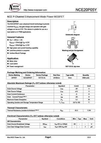
http //www.ncepower.com NCE20P05Y NCE P-Channel Enhancement Mode Power MOSFET Description The NCE20P05Y uses advanced trench technology to provide excellent R , low gate charge and operation with gate DS(ON) voltages as low as 2.5V. This device is suitable for use as a load switch or in PWM applications. Schematic diagram General Features V = -20V,I = -5A DS D R
nce20p05j.pdf
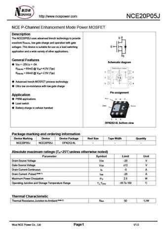
http //www.ncepower.com NCE20P05J NCE P-Channel Enhancement Mode Power MOSFET Description D The NCE20P05J uses advanced trench technology to provide excellent R , low gate charge and operation with gate DS(ON) G voltages .This device is suitable for use as a load switching application and a wide variety of other applications. S General Features Schematic diagram V = -20V,I = -
nce20p08j.pdf

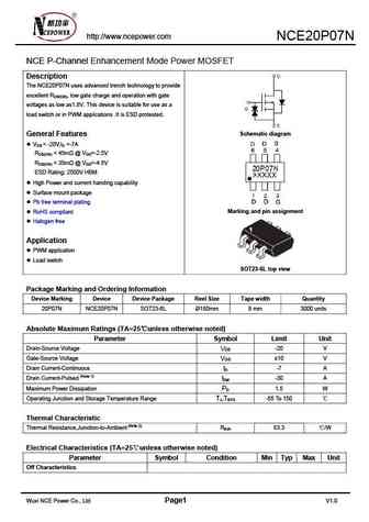
http //www.ncepower.com NCE20P08J NCE P-Channel Enhancement Mode Power MOSFET Description D The NCE20P08J uses advanced trench technology to provide excellent R , low gate charge and operation with gate DS(ON) G voltages .This device is suitable for use as a load switching application and a wide variety of other applications. S General Features Schematic diagram V = -20V,I = -
nce20p09s.pdf
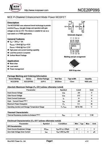
http //www.ncepower.com NCE20P09S NCE P-Channel Enhancement Mode Power MOSFET D1 D2 Description The NCE20P09S uses advanced trench technology to provide G1 G2 excellent R , low gate charge and operation with gate DS(ON) voltages as low as 2.5V. This device is suitable for use as a S1 S2 load switch or in PWM applications. Schematic diagram General Features V = -20V,I = -9A D
Otros transistores... NCE2013J, NCE2014ES, NCE2025I, NCE2025S, NCE2030U, NCE2090K, NCE20NP1006S, NCE20P05J, K2611, NCE20P07N, NCE20P08J, NCE20P09S, NCE20P10J, NCE20P85GU, NCE2301A, NCE2301B, NCE2301C
🌐 : EN ES РУ

Liste
Recientemente añadidas las descripciónes de los transistores:
MOSFET: FTF30P35D | FTF25N35DHVT | FTF15N35D | FTE15C35G | FTP02P15G | FTE02P15G | AKF30N5P0SX | AKF30N10S | AKF20P45D | CM4407 | CM3407 | CM3400 | SVF11N65F | SVF11N65T | FKBB3105 | EHBA036R1
Popular searches
2sd2560 | 2sc2078 transistor | bc558 datasheet | p75nf75 mosfet | ao4407a | mpsa06 datasheet | bc548 pinout | bdw94c