NCE3401BY MOSFET Equivalente. Reemplazo. Hoja de especificaciones. Principales características
Número de Parte: NCE3401BY
Tipo de FET: MOSFET
Polaridad de transistor: P
ESPECIFICACIONES MÁXIMAS
Pdⓘ - Máxima disipación de potencia: 1.3 W
|Vds|ⓘ - Voltaje máximo drenador-fuente: 30 V
|Vgs|ⓘ - Voltaje máximo fuente-puerta: 12 V
|Id|ⓘ - Corriente continua de drenaje: 4.4 A
Tjⓘ - Temperatura máxima de unión: 150 °C
CARACTERÍSTICAS ELÉCTRICAS
trⓘ - Tiempo de subida: 3.5 nS
Cossⓘ - Capacitancia de salida: 90.3 pF
RDSonⓘ - Resistencia estado encendido drenaje a fuente: 0.055 Ohm
Encapsulados: SOT-23
Búsqueda de reemplazo de NCE3401BY MOSFET
- Selecciónⓘ de transistores por parámetros
NCE3401BY datasheet
nce3401by.pdf
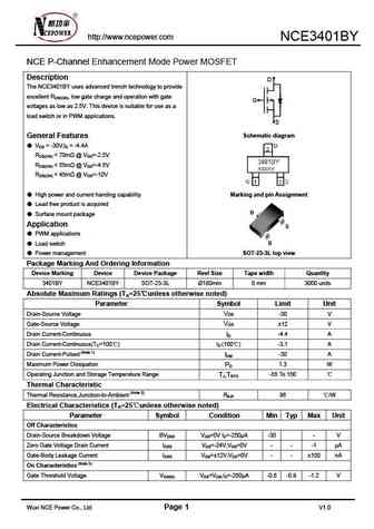
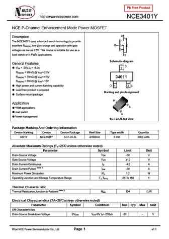
http //www.ncepower.com NCE3401BY NCE P-Channel Enhancement Mode Power MOSFET Description D The NCE3401BY uses advanced trench technology to provide excellent RDS(ON), low gate charge and operation with gate G voltages as low as 2.5V. This device is suitable for use as a load switch or in PWM applications. S Schematic diagram General Features VDS = -30V,ID = -4.4A RD
nce3401ay.pdf
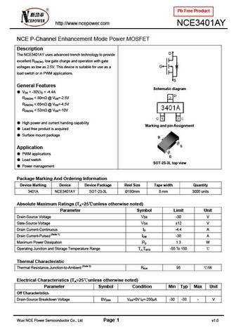
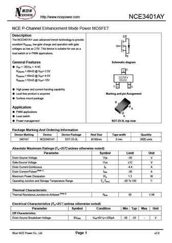
Pb Free Product http //www.ncepower.com NCE3401AY NCE P-Channel Enhancement Mode Power MOSFET Description D The NCE3401AY uses advanced trench technology to provide excellent RDS(ON), low gate charge and operation with gate G voltages as low as 2.5V. This device is suitable for use as a load switch or in PWM applications. S General Features Schematic diagram VDS = -30
nce3401a.pdf
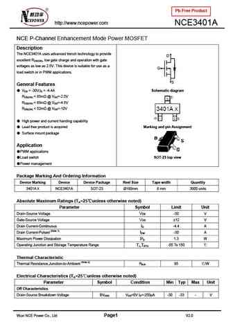
Pb Free Product http //www.ncepower.com NCE3401A NCE P-Channel Enhancement Mode Power MOSFET Description The NCE3401A uses advanced trench technology to provide D excellent RDS(ON), low gate charge and operation with gate voltages as low as 2.5V. This device is suitable for use as a G load switch or in PWM applications. S General Features VDS = -30V,ID = -4.4A Schematic
nce3401.pdf
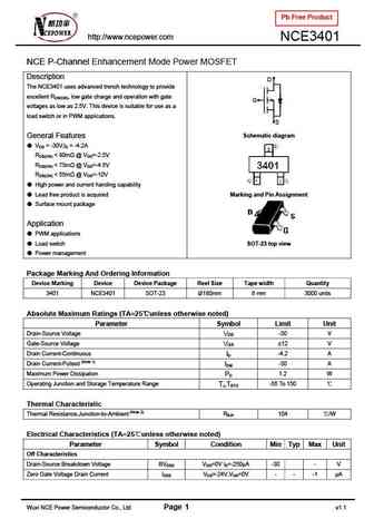
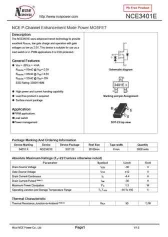
Pb Free Product http //www.ncepower.com NCE3401 NCE P-Channel Enhancement Mode Power MOSFET Description D The NCE3401 uses advanced trench technology to provide excellent RDS(ON), low gate charge and operation with gate G voltages as low as 2.5V. This device is suitable for use as a load switch or in PWM applications. S Schematic diagram General Features VDS = -30V,ID
Otros transistores... NCE30P55K, NCE30P55L, NCE30P60G, NCE30P85K, NCE3134, NCE3400E, NCE3400XY, NCE3401A, BS170, NCE3401E, NCE3401Y, NCE3402, NCE3402A, NCE3406AN, NCE3407A, NCE3407E, NCE3415E
History: AOP605
🌐 : EN ES РУ

Liste
Recientemente añadidas las descripciónes de los transistores:
MOSFET: FTF30P35D | FTF25N35DHVT | FTF15N35D | FTE15C35G | FTP02P15G | FTE02P15G | AKF30N5P0SX | AKF30N10S | AKF20P45D | CM4407 | CM3407 | CM3400 | SVF11N65F | SVF11N65T | FKBB3105 | EHBA036R1
Popular searches
2sc1815 datasheet | mj15015 | 13003 transistor datasheet | 2n3416 | bdx53c | k3563 | d882p | 2sb1560