NCE3401BY Datasheet. Specs and Replacement
Type Designator: NCE3401BY 📄📄
Type of Transistor: MOSFET
Type of Control Channel: P-Channel
Absolute Maximum Ratings
Pd ⓘ - Maximum Power Dissipation: 1.3 W
|Vds|ⓘ - Maximum Drain-Source Voltage: 30 V
|Vgs|ⓘ - Maximum Gate-Source Voltage: 12 V
|Id| ⓘ - Maximum Drain Current: 4.4 A
Tj ⓘ - Maximum Junction Temperature: 150 °C
Electrical Characteristics
tr ⓘ - Rise Time: 3.5 nS
Cossⓘ - Output Capacitance: 90.3 pF
RDSonⓘ - Maximum Drain-Source On-State Resistance: 0.055 Ohm
Package: SOT-23
📄📄 Copy
NCE3401BY substitution
- MOSFET ⓘ Cross-Reference Search
NCE3401BY datasheet
nce3401by.pdf
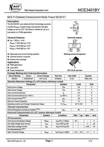
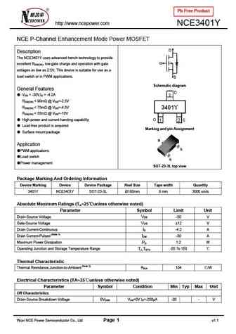
http //www.ncepower.com NCE3401BY NCE P-Channel Enhancement Mode Power MOSFET Description D The NCE3401BY uses advanced trench technology to provide excellent RDS(ON), low gate charge and operation with gate G voltages as low as 2.5V. This device is suitable for use as a load switch or in PWM applications. S Schematic diagram General Features VDS = -30V,ID = -4.4A RD... See More ⇒
nce3401ay.pdf
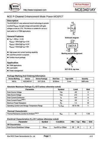
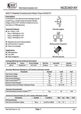
Pb Free Product http //www.ncepower.com NCE3401AY NCE P-Channel Enhancement Mode Power MOSFET Description D The NCE3401AY uses advanced trench technology to provide excellent RDS(ON), low gate charge and operation with gate G voltages as low as 2.5V. This device is suitable for use as a load switch or in PWM applications. S General Features Schematic diagram VDS = -30... See More ⇒
nce3401a.pdf
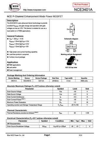
Pb Free Product http //www.ncepower.com NCE3401A NCE P-Channel Enhancement Mode Power MOSFET Description The NCE3401A uses advanced trench technology to provide D excellent RDS(ON), low gate charge and operation with gate voltages as low as 2.5V. This device is suitable for use as a G load switch or in PWM applications. S General Features VDS = -30V,ID = -4.4A Schematic... See More ⇒
nce3401.pdf
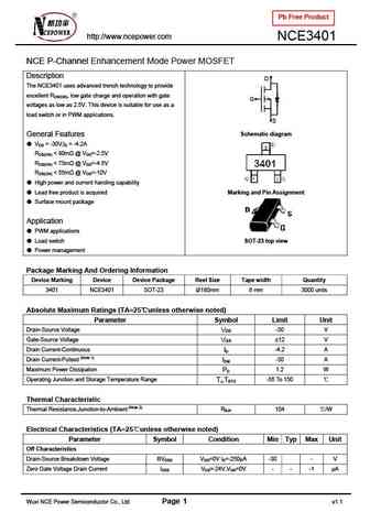
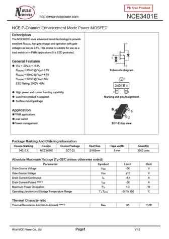
Pb Free Product http //www.ncepower.com NCE3401 NCE P-Channel Enhancement Mode Power MOSFET Description D The NCE3401 uses advanced trench technology to provide excellent RDS(ON), low gate charge and operation with gate G voltages as low as 2.5V. This device is suitable for use as a load switch or in PWM applications. S Schematic diagram General Features VDS = -30V,ID... See More ⇒
Detailed specifications: NCE30P55K, NCE30P55L, NCE30P60G, NCE30P85K, NCE3134, NCE3400E, NCE3400XY, NCE3401A, CS150N04A8, NCE3401E, NCE3401Y, NCE3402, NCE3402A, NCE3406AN, NCE3407A, NCE3407E, NCE3415E
Keywords - NCE3401BY MOSFET specs
NCE3401BY cross reference
NCE3401BY equivalent finder
NCE3401BY pdf lookup
NCE3401BY substitution
NCE3401BY replacement
Can't find your MOSFET? Learn how to find a substitute transistor by analyzing voltage, current and package compatibility
MOSFET Parameters. How They Affect Each Other
History: FDY300NZ | CI47N65 | NTGD3148NT1G | FDB86135
🌐 : EN ES РУ

LIST
Last Update
MOSFET: CS95118 | CS85105A | CS75N45 | CS72N12 | CS55N50 | CS48N75A | CS40N27 | MSQ60P04D | MSQ40P07D | MSQ30P40D
Popular searches
2sc1815 datasheet | mj15015 | 13003 transistor datasheet | 2n3416 | bdx53c | k3563 | d882p | 2sb1560